
FCO-9C-LN SMD 1409 Low Phase Noise CMOS Oscillator
100 MHz and 122.88 MHz reference-clock configurations for RF synthesizers, test instruments and communication clock paths. Select a 3.3 V CMOS interface and review the phase-noise requirements of your receiving circuit with FCom.
Contact FCom for the current product specification.
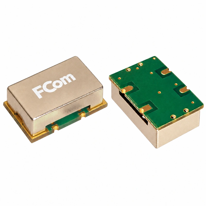
Design-in guidance: This is a fixed-frequency XO configuration. Check the receiver’s CMOS input limits, capacitive load and phase-noise mask. A clock loop that requires direct voltage tuning needs a VCXO configuration.
Reference-clock selection for low-noise systems
Start with the exact carrier frequency and electrical interface. Then match source phase noise and frequency stability to the requirements of the complete clock path.
100 and 122.88 MHz
Choose the fixed output frequency required by the receiver or synthesizer reference input. Evaluate each frequency using its own phase-noise data.
Single-ended CMOS output
Review the receiver’s input thresholds, output loading and trace arrangement. Supply voltage and output high/low levels are separate electrical specifications.
Define the stability budget
Specify initial frequency error, temperature variation, supply and load effects. Agree the aging allowance and duration in the final product specification.
Phase noise and RMS phase jitter
Send FCom your phase-noise mask at the relevant offset frequencies. For integrated RMS phase jitter, specify the integration band and carrier frequency together with supply, temperature and output load. Frequency accuracy in ppm and timing noise require separate evaluation.
- Carrier: 100 / 122.88 MHz
- Offset: 10 Hz to 1 MHz, as required
- Application-specific integration band
- Supply, temperature and load
- Spurious limits
Match the reference to your clock architecture
The following selection configurations use 3.3 V CMOS output, a ±25 ppm stability target and −40 to +85°C operation. Receiver compatibility and the final noise budget determine suitability.
100 MHz RF synthesizer reference
Use a 100 MHz fixed reference at a compatible CMOS reference input in an RF frequency-synthesis chain.
Recommend Parts FCO9C33CDYLN-100MHz100 MHz configurationDesign consideration: Review phase noise at offsets inside and outside the PLL loop bandwidth, reference spurs and input-level limits. Confirm any coupling or level translation required by the synthesizer.
100 MHz test-instrument clock
Select a 100 MHz reference for an instrument’s internal timing or synthesis stage where the receiving circuit accepts CMOS.
Recommend Parts FCO9C33CDYLN-100MHz100 MHz configurationDesign consideration: Set separate limits for phase noise, absolute frequency error and aging. A CMOS output requires an appropriate interface to drive a 50 Ω instrument input.
122.88 MHz radio reference
Evaluate a 122.88 MHz reference for a radio clock tree or frequency-synthesis architecture that requires this exact input frequency.
Recommend Parts FCO9C33CDYLN-122.88MHz122.88 MHz configurationDesign consideration: Check receiver input limits and total clock-path noise. Systems requiring tighter absolute frequency accuracy or synchronization need additional clock-architecture review.
122.88 MHz converter-clock PLL reference
Provide a fixed reference to a compatible clock PLL that generates the sampling clocks for an ADC or DAC signal chain.
Recommend Parts FCO9C33CDYLN-122.88MHz122.88 MHz configurationDesign consideration: Budget reference noise, PLL transfer characteristics and clock-distribution noise against the converter’s sampling-clock requirements. Specify the integration band used for jitter evaluation.
High-Speed Data Conversion, FPGA & SerDes Application Guide (PDF)
For other supply-voltage requirements, please contact our sales team.
Review phase noise, jitter and clock options
Explore the relevant system-level application areas, then review phase noise, jitter and oscillator options for your receiving circuit.
Compare reference-clock architectures by frequency stability, output format and tuning requirements.
Understand spot phase noise and integrated RMS phase jitter when defining a clock specification.
Review other output interfaces and clock families for your receiver and timing architecture.
Frequently Asked Questions
Which part number should I select for each frequency?
Select FCO9C33CDYLN-100MHz for a 100 MHz reference or FCO9C33CDYLN-122.88MHz for a 122.88 MHz reference. Both selection configurations use a 3.3 V supply, single-ended CMOS output and a −40 to +85°C operating temperature range.
Does 3.3 V specify the supply or the output voltage?
3.3 V is the nominal supply voltage. The CMOS output high and low levels, drive capability, load and permitted supply tolerance must be checked separately in the selected part’s electrical specification.
Is FCO-9C-LN a voltage-controlled oscillator?
FCO-9C-LN is a fixed-frequency XO configuration. If your loop requires control-voltage tuning, contact FCom to select a suitable VCXO with the required pull range and tuning characteristics.
How should the ±25 ppm stability target be specified?
±25 ppm is the selection target for the configurations shown. Request a frequency-error budget covering initial accuracy, operating temperature, supply and load variation, and specify whether aging is included and over what period. The final product specification defines the guaranteed limits.
How should phase noise and integrated jitter be compared?
Compare phase noise at the same carrier frequency and offset frequencies under matched test conditions. Compare RMS phase jitter using the same integration band, supply voltage, temperature and output load. Review 100 MHz and 122.88 MHz results separately.
Can the CMOS output directly drive a 50 Ω input?
Check the specified output load and receiving input before connecting them. A 50 Ω termination can impose a substantially different load from a CMOS input. Ask FCom to review buffering, attenuation, coupling or level translation for your circuit.
What package and PCB information should I request?
SMD 1409 denotes the nominal 9 × 14 mm SMD package class used for this series. Obtain the part-specific mechanical drawing, height, pad layout, pin functions and assembly conditions before finalizing the PCB footprint.
What information does FCom need for design-in support?
Send the full part number, receiver type, supply voltage, operating temperature, stability and aging requirements, output loading, phase-noise mask and jitter integration band. Include the clock-tree architecture and any supply-current or startup constraints. For other supply-voltage requirements, please contact our sales team.