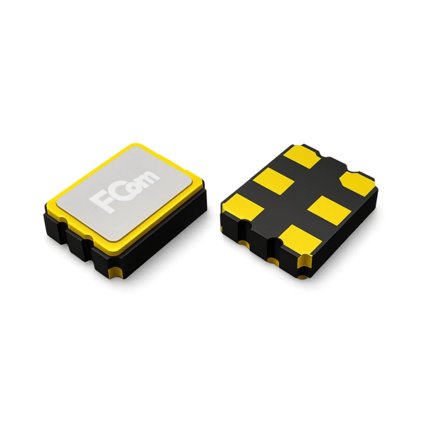
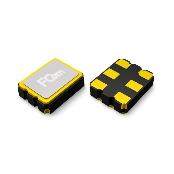
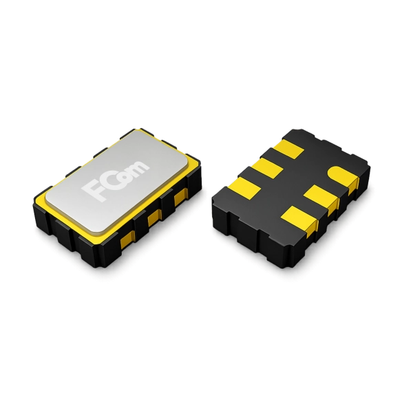
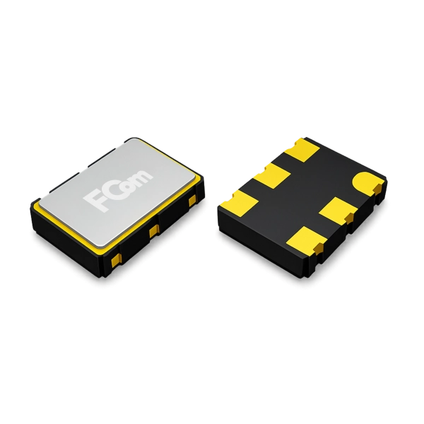
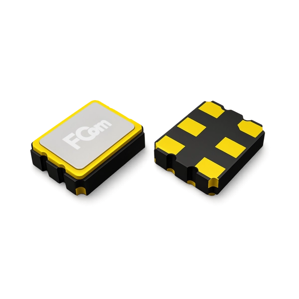
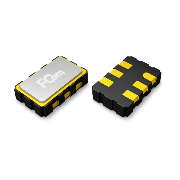
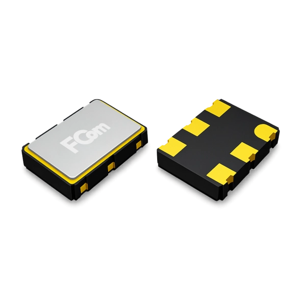
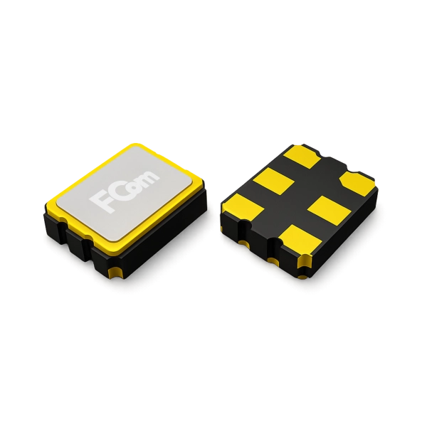
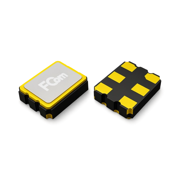
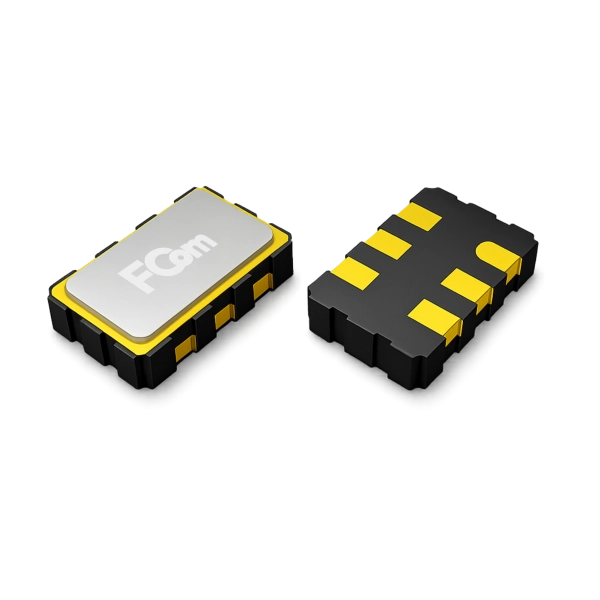
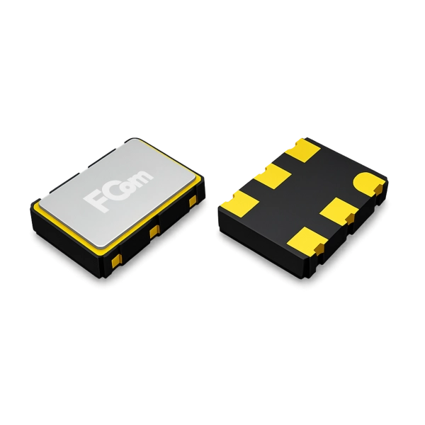
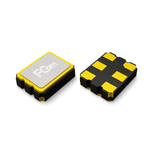
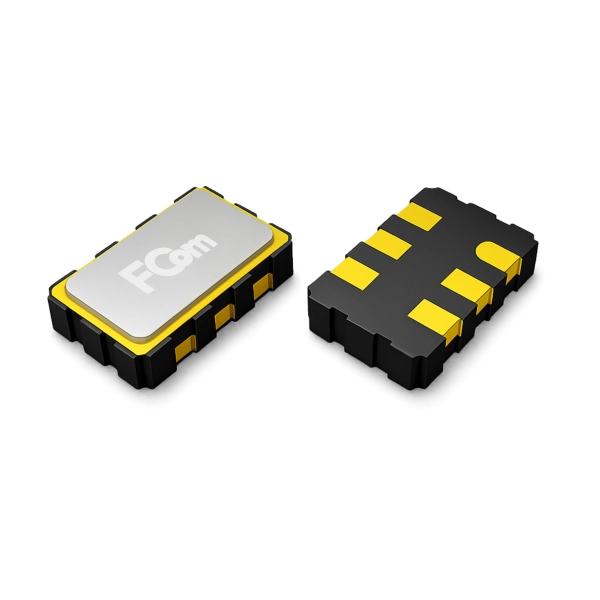
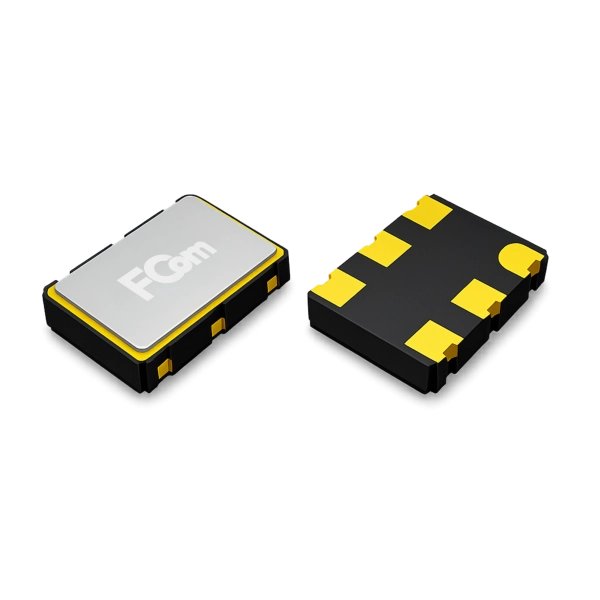
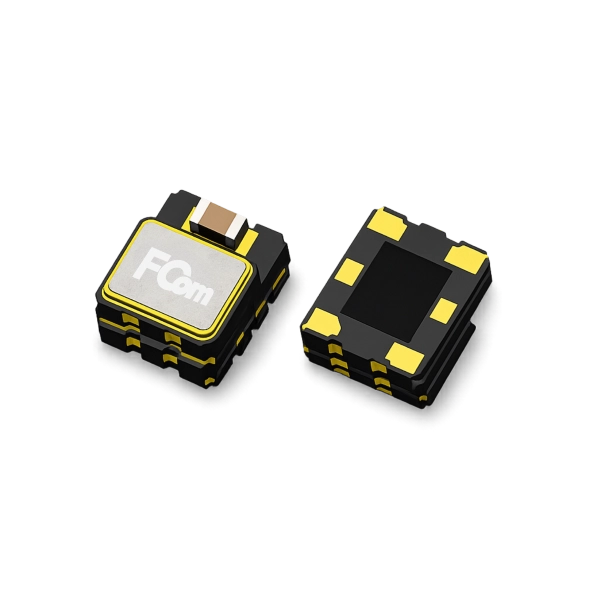
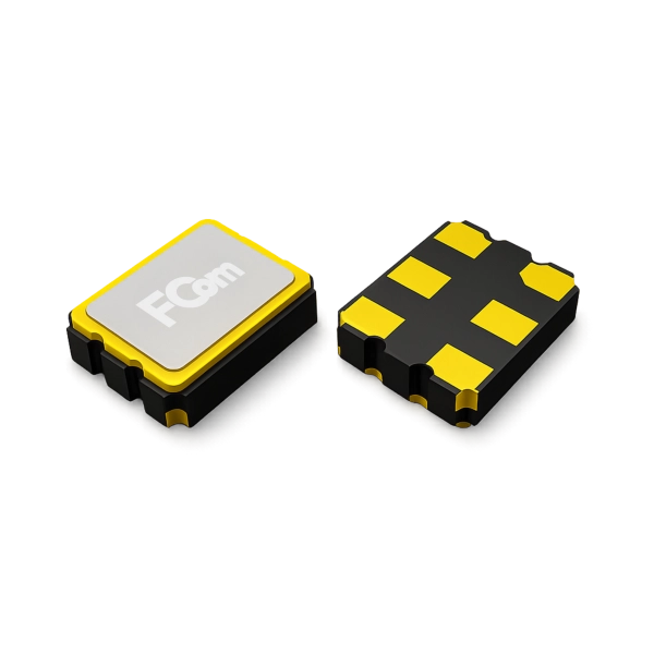
Low Jitter Series

Low-Jitter Oscillators for High-Speed Signal Integrity

FCom low-jitter XO, TCXO and VCXO solutions provide clean reference clocks for high-speed serial links, optical modules, data-center networking and telecom systems. Select by RMS phase jitter, integration bandwidth, output logic, frequency and operating temperature.

Choose the Right Clock Architecture

Ultra-Low-Jitter Differential XO

Clean differential reference clocks for applications with the tightest jitter budgets.
Down to 50 fs RMS

Standard Differential XO

Balanced jitter, interface flexibility and package options for high-speed digital clock distribution.
Down to 150 fs RMS

Low-Jitter CMOS XO

Solutions for processors, controllers and digital systems that do not require differential signaling.
Down to 0.6 ps RMS

Compensated & Tunable Clocks

Clocks for systems that require frequency stability or tuning in addition to low timing noise.
TCXO and VCXO Options
Measured Under Defined Test Conditions
Low-jitter performance is evaluated through phase-noise measurement and integrated RMS phase-jitter analysis under defined carrier-frequency and offset-range conditions.
*Production verification and test documentation are available according to product series and project requirements.

Jitter Is More Than One Number

A jitter value is meaningful only when the measurement method and test conditions are defined.
RMS Phase Jitter
Integration Bandwidth
Carrier Frequency
Output Logic
Load Conditions

Low-Jitter Clock Oscillator Portfolio

Compare standard clock solutions, review technical data, or submit your jitter and interface requirements for engineering support.
*All jitter data is integrated RMS phase jitter, 12 kHz to 20 MHz
PictureSeriesPackageFrequency RangeSupply VoltageTightest StabilityTemp. RangeOutputInput CurrentJitterMountContact
Low Jitter Oscillator
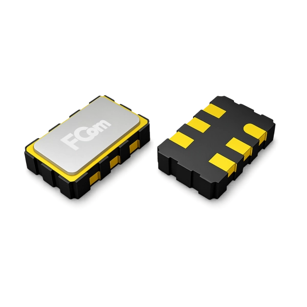
Differential oscillator FCO-2L-UJ FCO-2L-UJ 2520 6-SMD100 - 220 MHz1.8 V, 2.5 V, 3.3 V±20 ppm-40 to +125℃LVPECL, LVDS, HCSL25 - 65 mA50 fsSMD Inquiry
Differential oscillator FCO-3L-UJ FCO-3L-UJ 3225 6-SMD100 - 220 MHz1.8 V, 2.5 V, 3.3 V±20 ppm-40 to +125℃LVPECL, LVDS, HCSL25 - 65 mA50 fsSMD Inquiry
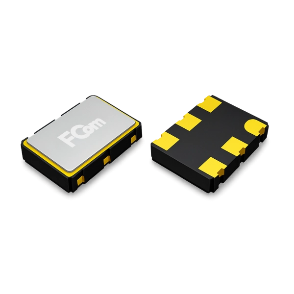
Differential oscillator FCO-5L-UJ FCO-5L-UJ 5032 6-SMD100 - 220 MHz1.8 V, 2.5 V, 3.3 V±20 ppm-40 to +125℃LVPECL, LVDS, HCSL25 - 65 mA50 fsSMD Inquiry
Differential oscillator FCO-7L-UJ FCO-7L-UJ 7050 6-SMD70 - 170 MHz2.5 V, 3.3 V±25 ppm-40 to +85℃LVPECL75 mA100 fsSMD Inquiry
Programmable oscillator FCO-3P-UJ FCO-3P-UJ 3225 6-SMD10 - 250 MHz2.5 V, 3.3 V±25 ppm-40 to +105℃CMOS45 - 50 mA0.8 psSMD Inquiry
Programmable oscillator FCO-5P-UJ FCO-5P-UJ 5032 6-SMD10 - 250 MHz2.5 V, 3.3 V±25 ppm-40 to +85℃CMOS30 mA0.6 psSMD Inquiry
Programmable oscillator FCO-7P-UJ FCO-7P-UJ 7050 6-SMD10 - 250 MHz2.5 V, 3.3 V±25 ppm-40 to +105℃CMOS30 mA0.6 psSMD Inquiry
View All Crystal Oscillators products
Differential Oscillator
Differential crystal oscillator FCO-2L FCO-2L 2520 6-SMD13.5 - 220 MHz1.8 V, 2.5 V, 3.3 V±25 ppm-40 to +105℃LVPECL, LVDS, HCSL20 - 55 mA0.15 psSMD Inquiry
Differential crystal oscillator FCO-3L FCO-3L 3225 6-SMD13.5 - 220 MHz1.8 V, 2.5 V, 3.3 V±25 ppm-40 to +105℃LVPECL, LVDS, HCSL20 - 55 mA0.15 psSMD Inquiry
Differential crystal oscillator FCO-5L FCO-5L 5032 6-SMD13.5 - 220 MHz1.8 V, 2.5 V, 3.3 V±25 ppm-40 to +105℃LVPECL, LVDS, HCSL20 - 55 mA0.15 psSMD Inquiry
Differential crystal oscillator FCO-7L FCO-7L 7050 6-SMD13.5 - 220 MHz1.8 V, 2.5 V, 3.3 V±25 ppm-40 to +105℃LVPECL, LVDS, HCSL20 - 55 mA0.15 psSMD Inquiry
Differential crystal oscillator FCO-3L-PG FCO-3L-PG 3225 6-SMD10 - 1500 MHz2.5 V, 3.3 V±25 ppm-40 to +105℃LVPECL, LVDS35 - 50 mA0.6 psSMD Inquiry
Differential crystal oscillator FCO-5L-PG FCO-5L-PG 5032 6-SMD10 - 1500 MHz2.5 V, 3.3 V±25 ppm-40 to +105℃LVPECL, LVDS50 mA0.6 psSMD Inquiry
Differential crystal oscillator FCO-7L-PG FCO-7L-PG 7050 6-SMD10 - 1500 MHz2.5 V, 3.3 V±25 ppm-40 to +105℃LVPECL, LVDS50 mA0.6 psSMD Inquiry
View All Crystal Oscillators products
PictureSeriesPackageFrequency RangeSupply VoltageTightest StabilityTemp. RangeOutputPullability (VCTCXO)dBc/Hz @100 HzdBc/Hz @1 kHzdBc/Hz @10 kHzMounting TypeContact
Low Jitter TCXO
TCXO FVT-3S-LJ FVT-3S-LJ 3225 6-SMD10 - 1500 MHz2.5 V, 3.3 V±1 ppm-40 to +85℃LVPECL, LVDS, CMOS/-107-111-114SMD Inquiry
View All TCXO products
PictureSeriesPackageFrequency RangeSupply VoltageTightest StabilityTemp. RangeOutputPullability OptionsdBc/Hz @100 HzdBc/Hz @1 kHzdBc/Hz @10 kHzdBc/Hz @100 kHzMounting TypeContact
Differential VCXO
VCXO FVC-3L-PG FVC-3L-PG 3225 6-SMD10 - 1500 MHz2.5 V, 3.3 V±25 ppm to ±50 ppm-40 to +105℃LVPECL, LVDS±50 ppm to ±150 ppm/-107-111-114SMD Inquiry
VCXO FVC-5L-PG FVC-5L-PG 5032 6-SMD10 - 1500 MHz2.5 V, 3.3 V±25 ppm to ±50 ppm-40 to +105℃LVPECL, LVDS±50 ppm (APR)-70-95-105/SMD Inquiry
VCXO FVC-7L-PG FVC-7L-PG 7050 6-SMD10 - 1500 MHz2.5 V, 3.3 V±25 ppm to ±50 ppm-40 to +105℃LVPECL, LVDS±50 ppm (APR)-70-95-105/SMD Inquiry
View All VCXO products
For complete mechanical drawings and ordering codes, contact to download the product catalog.

Technical Applications

Explore how FCom ultra-low jitter series integrate seamlessly into your specific system architectures to secure signal integrity.
Need help selecting the right stability grade?
image-172
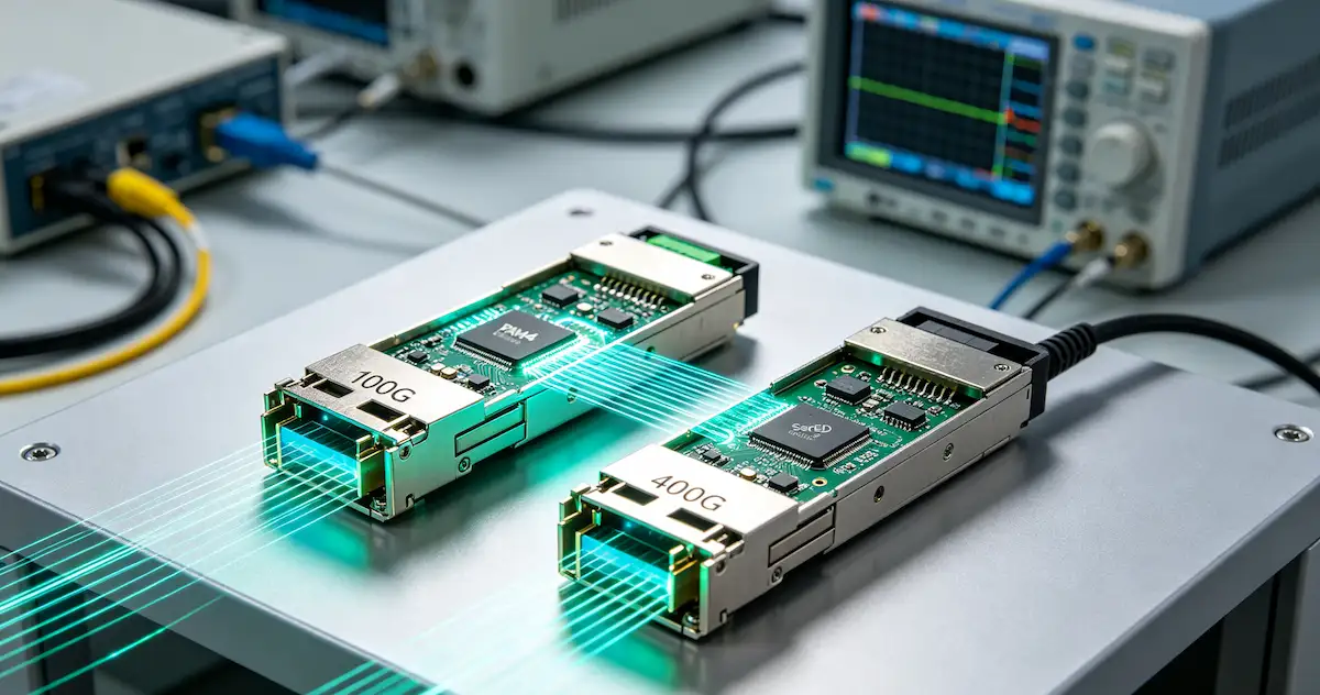
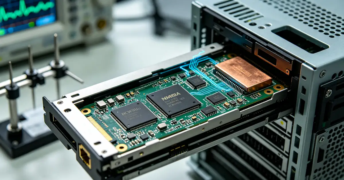
100G / 400G Optical Modules
Design Challenge
 
Keeping optical PHY and SerDes clock jitter within the link budget.
 
Recommended Solution
 
Match a differential XO to the receiver’s jitter mask and budget.
 
Key Parameters
 
  • RMS Jitter & Integration Band
  • Receiver Phase-Noise Mask
  • Clock-Tree Additive Jitter
  • Output Interface
  • Exact Reference Frequency


View Application Guide (PDF) →

image-173
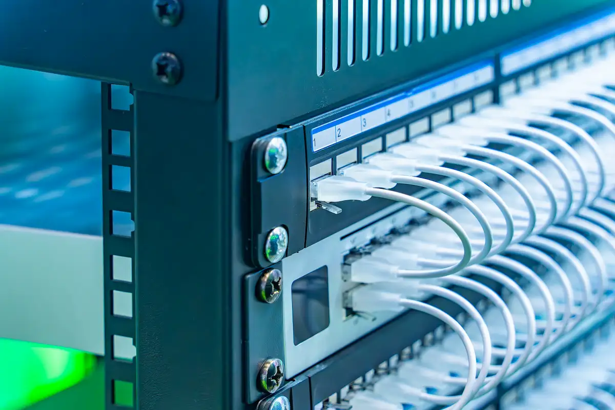
Data Center Switches & SmartNICs
Design Challenge
 
Controlling clock jitter from supply noise and dense-board coupling.
 
Recommended Solution
 
Use a low-jitter differential XO within the total clock-path budget.
 
Key Parameters
 
  • RMS Jitter & Integration Band
  • Clock-Tree Additive Jitter
  • Supply-Noise Sensitivity
  • Output Interface & Termination
  • Clock-Distribution Topology


View Application Guide (PDF) →

image-174
PCIe Server & Accelerator Platforms
Design Challenge
 
Meeting 100 MHz PCIe jitter limits across host and endpoint paths.
 
Recommended Solution
 
Use HCSL where a local XO is required; check the PCIe jitter mask.
 
Key Parameters
 
  • PCIe Generation & Jitter Mask
  • Common Clock / SRNS / SRIS
  • SSC Mode
  • HCSL Interface & Termination
  • Clock-Path Additive Jitter


View Application Guide (PDF) →

image-175
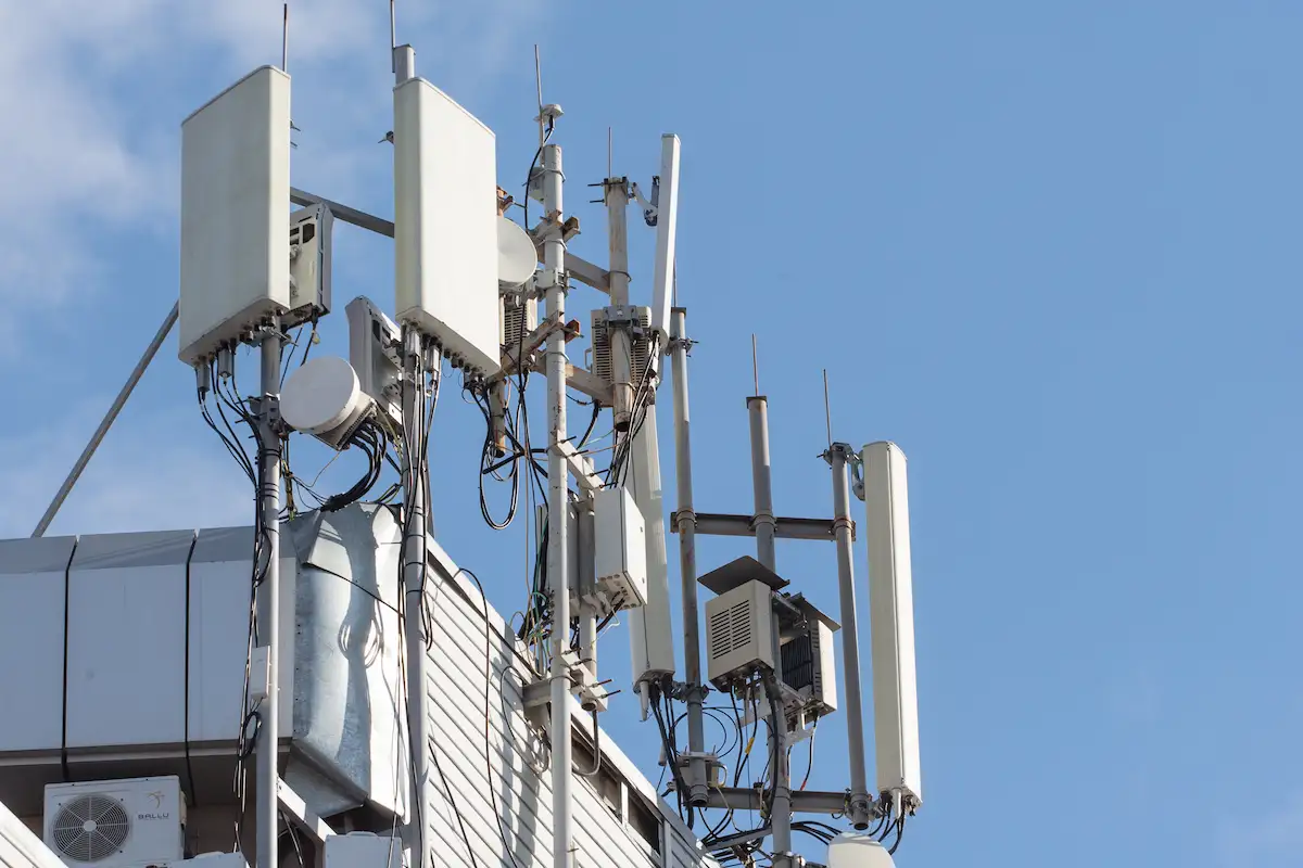
5G Radio & Converter Clocking
Design Challenge
 
Controlling radio and converter jitter through the full clock tree.
 
Recommended Solution
 
Use a low-jitter XO, or VCXO only when the clock loop needs tuning.
 
Key Parameters
 
  • Phase Noise & Spurious Limits
  • RMS Jitter & Integration Band
  • PLL Transfer & Additive Jitter
  • Exact Reference Frequency
  • Device-Clock / SYSREF Architecture


View Application Guide (PDF) →

Find the Right Low-Jitter Clock

Compare standard products, review technical specifications, or send us your clock requirements for engineering support.

STANDARD PRODUCTS

Compare Low-Jitter Clocks

Review available XO, TCXO and VCXO options by frequency, RMS phase jitter, output logic, package and supply voltage.

TECHNICAL RESOURCES

Download the Series Guide

Review available series, jitter specifications, phase-noise data, package drawings and ordering information.
ENGINEERING SUPPORT

Need a Custom Clock Specification?

Send us your target frequency, jitter budget, integration bandwidth, output logic, supply voltage and operating temperature for engineering review.

Contact Us Anytime

Drag & Drop Files, Choose Files to Upload

Contact Us Anytime

Drag & Drop Files, Choose Files to Upload

Contact Us Anytime

Drag & Drop Files, Choose Files to Upload