Clock Quality · Technical Guide
Phase noise and jitter describe clock timing fluctuations in different domains. Understanding their relationship helps engineers compare oscillators, interpret measurements and allocate noise budgets for RF, data-converter and digital systems.
FCom Fuji Crystal · Technical Guide
Phase noise and jitter explained
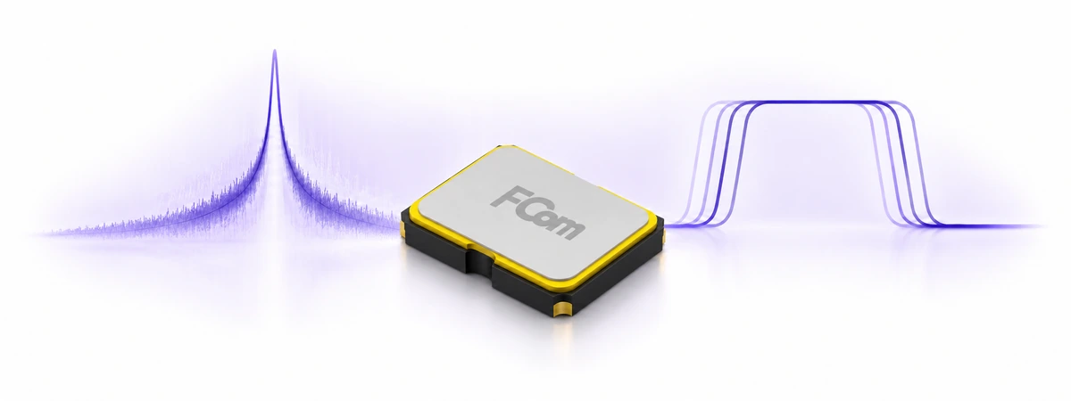
Phase noise is commonly specified as single-sideband noise density, L(f), in dBc/Hz at an offset from the carrier. The offset is the distance from the nominal oscillator frequency. A more negative value indicates lower noise density at that offset, under comparable conditions. Jitter expresses edge-timing variation, usually in picoseconds or femtoseconds. The two descriptions are related, but different jitter metrics apply different time-domain measurements. [6]
| Metric | What it describes | Required context |
|---|---|---|
| Spot phase noise | Noise density at one carrier offset. | dBc/Hz, carrier and offset frequency. |
| RMS phase jitter | Integrated phase fluctuations expressed as time. | Integration limits, filtering and spur treatment. |
| Period jitter | Variation of individual cycle lengths from the reference period. | RMS or peak-to-peak result and sample count. |
| Cycle-to-cycle jitter | Difference between adjacent cycle lengths. | Statistic, sample count and measurement method. |
| Time interval error | Edge displacement relative to a defined reference. | Reference recovery and observation interval. |
Period jitter, cycle-to-cycle jitter and RMS phase jitter are not interchangeable. A low value for one does not automatically establish a low value for another. [2]
Converting phase noise to RMS phase jitter
For small phase fluctuations and the usual symmetric single-sideband convention, integrate the linear noise ratio, then convert the RMS phase deviation into time. [1]
A = ∫f₁f₂ 10L(f)/10 df
σφ ≈ √(2A)
σt ≈ √(2A) / (2πf₀)
Here, f₀ is the carrier frequency in Hz; f₁ and f₂ are offset-frequency limits in Hz; σφ is RMS phase deviation in radians; and σt is RMS timing jitter in seconds.
The factor of two accounts for both sidebands. Do not apply it again to an already double-sideband phase-variance result. Convert dBc/Hz to linear units before integration; adding the displayed decibel values is incorrect.
Worked example
Assume a 100 MHz oscillator has an integrated single-sideband noise ratio A = 10−8, equivalent to −80 dBc, over a stated measurement band. Its calculated RMS phase jitter is:
√(2 × 10⁻⁸) / (2π × 100 × 106) ≈ 225 fs RMS
This is an illustrative calculation, not FCom measurement data. If the integrated noise power quadruples while carrier frequency stays fixed, RMS jitter doubles to approximately 450 fs.
Why integration bandwidth matters
An RMS phase-jitter figure summarizes only the included noise. A result integrated from 12 kHz to 20 MHz cannot be directly compared with one integrated from 10 Hz to 1 MHz. Neither band is a universal requirement for every system.
Choose the integration range from the receiver, converter or interface requirements. For RF converters, the relevant offsets can differ depending on whether the objective is signal-to-noise ratio, error vector magnitude or adjacent-channel performance. [3]
Where a system specifies a transfer function, apply its noise weighting rather than assuming a simple rectangular band. Also record whether discrete spurs are included. A spur-excluded result and a spur-inclusive result describe different measurement conditions.
What matters in your application
RF and frequency synthesis
Inspect the phase-noise curve across the offsets that affect the signal. Two clocks can have the same integrated jitter while distributing noise differently. A single RMS number can therefore conceal differences relevant to modulation quality or nearby interference. [3]
ADC sampling
For a sinusoidal input with small, uncorrelated sampling-time uncertainty, the jitter-limited signal-to-noise ratio is approximately:
SNRjitter = −20 log10(2πfinσt,total)
Here, fin is the analog input frequency, not the clock frequency. At 100 MHz input frequency and 200 fs total RMS sampling jitter, the calculated limit is approximately 78 dB. Quantization, thermal noise and distortion can reduce actual performance. [4]
Digital timing
Match the clock specification to the receiving device’s timing requirement. Period jitter can matter for cycle timing, while a serial interface may specify filtered phase jitter or time interval error. Retain the required measurement method instead of substituting whichever number looks smallest. [2]
Design and comparison checklist
- Normalize the comparison: Record carrier frequency, jitter type, integration range, spur handling, output format, load, supply and temperature.
- Preserve clock quality on the board: Follow the device’s decoupling, termination and layout guidance; separate sensitive clock routes from strong switching aggressors.
- Review the complete signal path: Include the oscillator, buffers, PLLs and receiving input in the assessment.
- Check the instrument: Its noise floor, timebase, bandwidth and acquisition settings must support the intended measurement.
- Separate typical and guaranteed values: Use the applicable limit for qualification and keep its conditions with the result.
Filtering is not automatically beneficial. A filter may remove out-of-band noise while reducing clock slew rate, increasing sensitivity to voltage noise at the receiver threshold. Evaluate the delivered waveform and system result. [4]
Likewise, PLL loop bandwidth trades off jitter, offset phase noise, lock time and spurs. Select it for the application rather than assuming that a narrower loop always produces a better clock. [5]
Frequently asked questions
Can one phase-noise point predict RMS jitter?
No. Conversion requires the noise across the specified integration range and the carrier frequency.
Does better ppm stability guarantee lower jitter?
No. Frequency tolerance, temperature stability and aging address different behavior. Evaluate phase-noise and jitter specifications separately.
Can RMS jitter be converted directly to peak-to-peak jitter?
There is no universal multiplier. The relationship depends on the noise distribution and the observation length or probability criterion. [2]
Does temperature compensation guarantee lower phase noise?
No. Temperature compensation controls frequency variation with temperature. Confirm phase-noise performance at the relevant offsets and operating conditions.
Discuss your clock requirements with FCom
Send your frequency, output format, supply, temperature range and noise limits to FCom@fujicrystal.com. Include the jitter definition, integration band and receiving-device requirements so we can review the relevant oscillator specifications with you.
Technical references
- Analog Devices. MT-008: Converting Oscillator Phase Noise to Time Jitter (PDF).
- SiTime. AN10007: Clock Jitter Definitions and Measurement Methods.
- Texas Instruments. SSZTAK9: RF sampling clock phase noise and integration limits.
- Texas Instruments. SSZTBT2: Sampling-clock jitter, SNR and filtering considerations.
- Texas Instruments. SSZTB85: PLL loop-bandwidth trade-offs.
- Analog Devices. Clock (CLK) Jitter and Phase Noise Conversion.