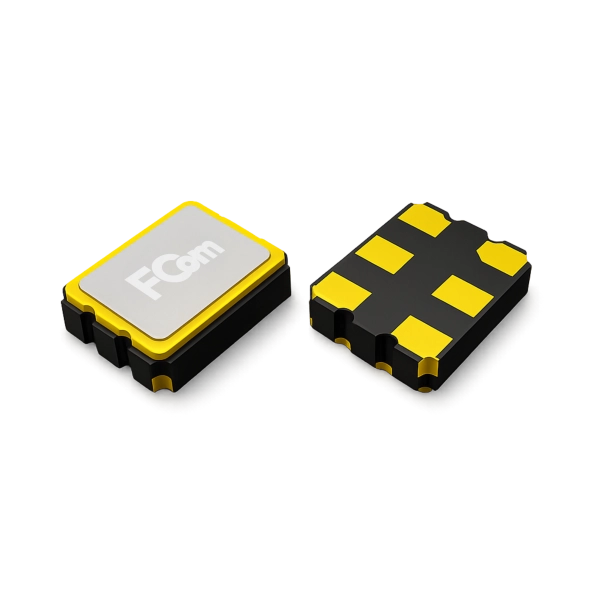
Differential Output Series

High-Frequency Clocking with Common-Mode Noise Immunity

FCom differential XO and VCXO solutions provide complementary clock outputs for high-speed networking, PCIe, optical communication and computing systems. Select by receiver interface, output frequency, RMS phase jitter, supply voltage, package and termination requirements.

Choose the Right Differential Interface

LVPECL
High-Swing Differential Output
For high-speed clock inputs requiring strong differential swing and low timing noise.
LVDS
Low-Swing Differential Output
For power-conscious systems requiring broad receiver compatibility and simple differential termination.
HCSL
PCIe-Oriented Clock Output
For PCIe and computing platforms requiring a current-steering differential reference clock.
Measured Under Defined Load Conditions
Differential output performance is evaluated under defined supply, load and termination conditions to verify output swing, duty cycle and complementary waveform behavior.
*Production verification scope and additional test documentation are available according to product series and project requirements.

How Differential Outputs Are Specified

A differential output is defined by more than its logic name. Receiver levels, output swing and termination must be evaluated together.
Differential Output Swing
Common-Mode Voltage
Termination and Coupling
Rise and Fall Time
Duty Cycle and Output Skew

Differential Output Oscillator Portfolio

Compare differential XO and VCXO solutions by frequency, output logic, RMS phase jitter, supply voltage, package and operating temperature. Confirm receiver compatibility and termination requirements in the individual datasheet.
*All jitter data is integrated RMS phase jitter, 12 kHz to 20 MHz
PictureSeriesPackageFrequency RangeSupply VoltageTightest StabilityTemp. RangeOutputInput CurrentJitterMountContact
Differential Oscillator
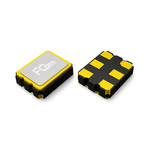
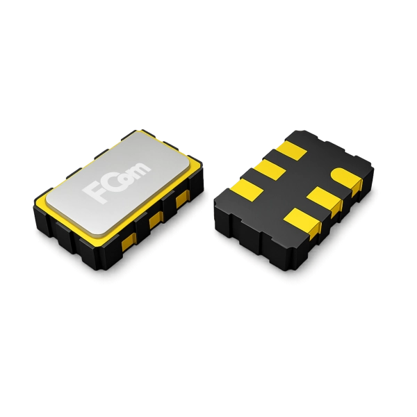
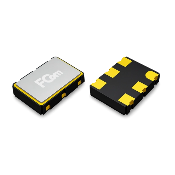
Differential crystal oscillator FCO-2L FCO-2L 2520 6-SMD13.5 - 220 MHz1.8 V, 2.5 V, 3.3 V±25 ppm-40 to +125℃LVPECL, LVDS, HCSL20 - 55 mA0.15 psSMD Inquiry
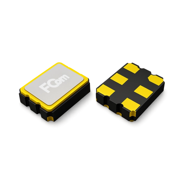
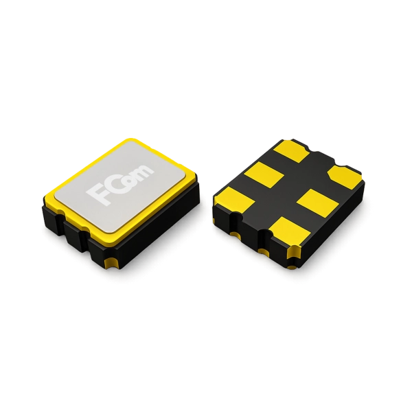
Differential crystal oscillator FCO-3L FCO-3L 3225 6-SMD13.5 - 220 MHz1.8 V, 2.5 V, 3.3 V±25 ppm-40 to +125℃LVPECL, LVDS, HCSL20 - 55 mA0.15 psSMD Inquiry
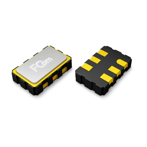
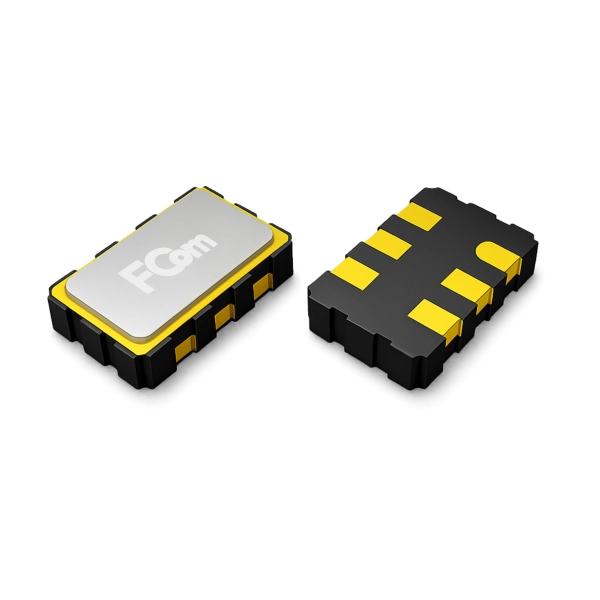
Differential crystal oscillator FCO-5L FCO-5L 5032 6-SMD13.5 - 220 MHz1.8 V, 2.5 V, 3.3 V±25 ppm-40 to +125℃LVPECL, LVDS, HCSL20 - 55 mA0.15 psSMD Inquiry
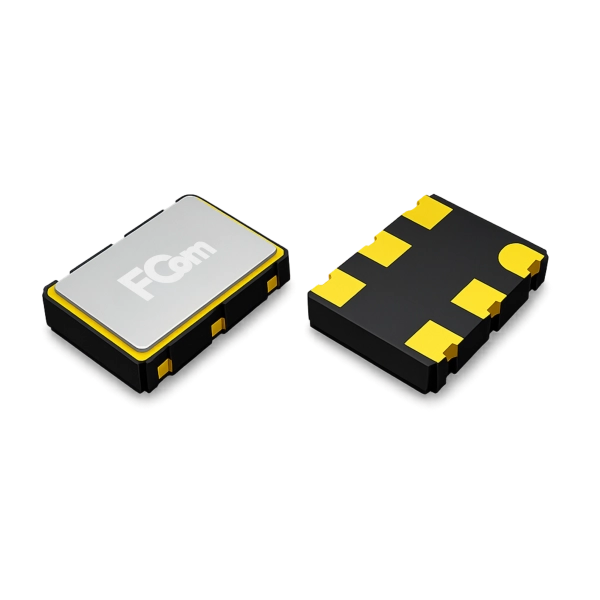
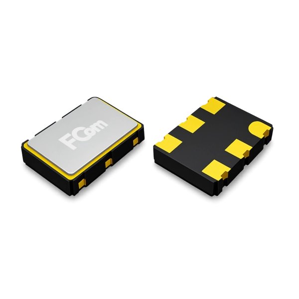
Differential crystal oscillator FCO-7L FCO-7L 7050 6-SMD13.5 - 220 MHz1.8 V, 2.5 V, 3.3 V±25 ppm-40 to +125℃LVPECL, LVDS, HCSL20 - 55 mA0.15 psSMD Inquiry
Differential crystal oscillator FCO-3L-PG FCO-3L-PG 3225 6-SMD10 - 1500 MHz2.5 V, 3.3 V±25 ppm-40 to +105℃LVPECL, LVDS35 - 50 mA0.6 psSMD Inquiry
Differential crystal oscillator FCO-5L-PG FCO-5L-PG 5032 6-SMD10 - 1500 MHz2.5 V, 3.3 V±25 ppm-40 to +85℃LVPECL, LVDS50 mA0.6 psSMD Inquiry
Differential crystal oscillator FCO-7L-PG FCO-7L-PG 7050 6-SMD10 - 1500 MHz2.5 V, 3.3 V±25 ppm-40 to +85℃LVPECL, LVDS50 mA0.6 psSMD Inquiry
View All Crystal Oscillators products
PictureSeriesPackageFrequency RangeSupply VoltageTightest StabilityTemp. RangeOutputPullability OptionsdBc/Hz @100 HzdBc/Hz @1 kHzdBc/Hz @10 kHzdBc/Hz @100 kHzMounting TypeContact
Differential VCXO
VCXO FVC-3L-PG FVC-3L-PG 3225 6-SMD10 - 1500 MHz2.5 V, 3.3 V±25 ppm to ±50 ppm-40 to +105℃LVPECL, LVDS±50 ppm to ±150 ppm/-107-111-114SMD Inquiry
VCXO FVC-5L-PG FVC-5L-PG 5032 6-SMD10 - 1500 MHz2.5 V, 3.3 V±25 ppm to ±50 ppm-40 to +105℃LVPECL, LVDS±50 ppm (APR)-70-95-105/SMD Inquiry
VCXO FVC-7L-PG FVC-7L-PG 7050 6-SMD10 - 1500 MHz2.5 V, 3.3 V±25 ppm to ±50 ppm-40 to +105℃LVPECL, LVDS±50 ppm (APR)-70-95-105/SMD Inquiry
View All VCXO products
For complete mechanical drawings and ordering codes, contact to download the product catalog.

Technical Applications

Applications where output compatibility, clock jitter and termination directly affect timing margin.
Need help selecting the right differential output mode?
image-184
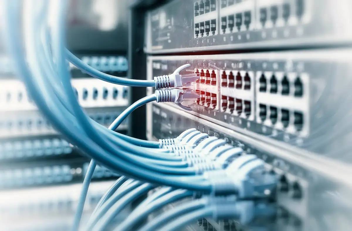
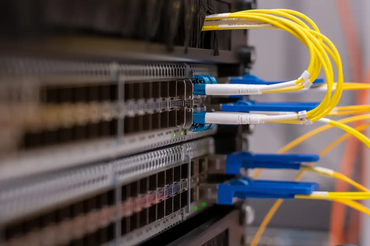
Network Switches & Routers
Design Challenge
 
Matching switch and router clocks to differential receiver inputs.
 
Recommended Solution
 
Match an LVDS or LVPECL XO to receiver levels and termination.
 
Key Parameters
 
  • Output Logic
  • Differential Output Swing
  • Receiver Common-Mode Range
  • Termination & Coupling
  • Rise/Fall Time


View Application Guide (PDF) →

image-185
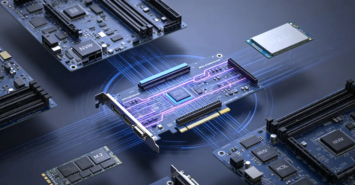
PCs & PCIe Expansion
Design Challenge
 
Matching PC and PCIe clocks to the receiver and clock architecture.
 
Recommended Solution
 
Use an HCSL XO only where a local 100 MHz clock source is required.
 
Key Parameters
 
  • HCSL Interface Type
  • Output Swing & Common Mode
  • Termination & Load
  • Clock Mode & SSC
  • Rise/Fall Time & Duty Cycle


View Application Guide (PDF) →

image-186
Optical Modules
Design Challenge
 
Matching optical clock inputs within module size and power limits.
 
Recommended Solution
 
Match an LVDS or LVPECL XO to input levels, jitter and power limits.
 
Key Parameters
 
  • Output Logic & Swing
  • Common Mode & Coupling
  • Receiver Termination
  • Supply Voltage & Current
  • Package Size & Height


View Application Guide (PDF) →

image-187
FPGA & SerDes Clocking
Design Challenge
 
Matching fixed or tunable references to FPGA and SerDes inputs.
 
Recommended Solution
 
Use a differential XO, or VCXO only for a loop that needs tuning.
 
Key Parameters
 
  • Output Swing & Common Mode
  • Termination & Coupling
  • Exact Reference Frequency
  • Pull Range / APR (VCXO)
  • Control Voltage (VCXO)


View Application Guide (PDF) →

Find the Right Differential Clock

Compare standard products, review interface specifications, or send us your receiver requirements for engineering support.

STANDARD PRODUCTS

Compare Differential Oscillators

Review available XO and VCXO series by frequency, output logic, jitter, voltage and package.

TECHNICAL RESOURCES

Download the Series Guide

Review output options, electrical specifications, package drawings and ordering information.
ENGINEERING SUPPORT

Need Help Matching the Receiver?

Send us your receiver part number, frequency, output interface, voltage and jitter requirements.

Contact Us Anytime

Drag & Drop Files, Choose Files to Upload

Contact Us Anytime

Drag & Drop Files, Choose Files to Upload

Contact Us Anytime

Drag & Drop Files, Choose Files to Upload