Timing fundamentals
By FCom Fuji Crystal
A crystal oscillator turns power from a DC supply into a periodic electrical signal. A quartz resonator selects a narrow frequency region, while active circuitry replaces the energy lost during vibration and delivers the clock signal.
Start here to understand the operating principle. For detailed specification and interface checks, continue to the quartz crystal oscillator parameters guide.
Is a quartz crystal the same as an oscillator?
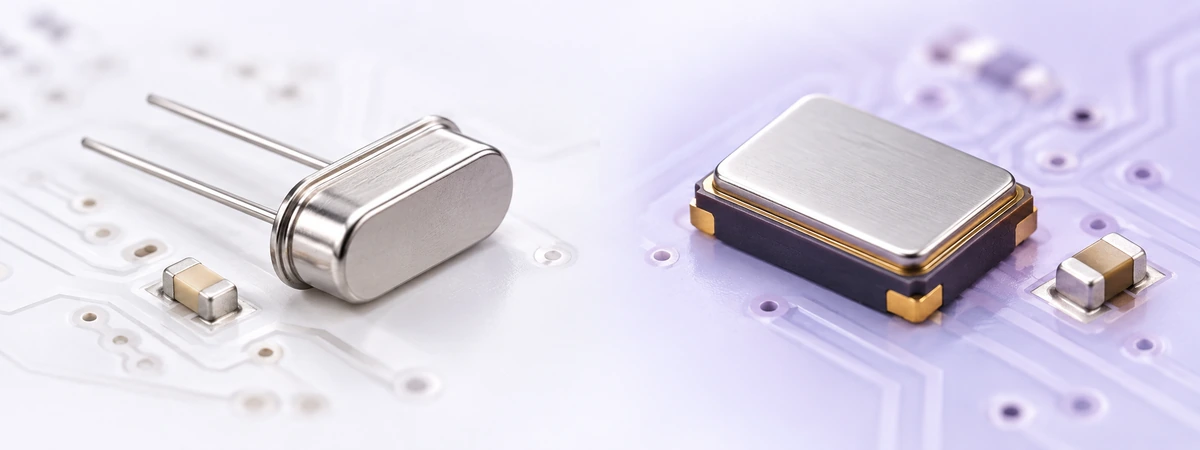
A crystal unit, often labelled XTAL, needs an external active circuit. A packaged oscillator includes that circuitry. Similar package dimensions do not establish electrical compatibility: identify the device from its pinout and datasheet.
| Device | Inside the device | Board connection |
|---|---|---|
| Quartz crystal | Passive quartz resonator and electrodes | Compatible oscillator pins and the specified loading network |
| Oscillator module | Resonator, active circuit and output stage | Supply, decoupling and a compatible external-clock input |
How does oscillation start and continue?
Quartz couples electrical and mechanical behavior through the piezoelectric effect. An electric field deforms it; deformation produces charge. An alternating excitation can therefore drive a mechanical resonance. The supply powers the amplifier that compensates for resonator losses.[1]
- Initiation: noise and power-on transients create a small signal.
- Growth: at the intended mode, reinforcing feedback and small-signal loop gain above one let the signal build.
- Steady operation: circuit nonlinearities or amplitude regulation reduce the effective loop gain to unity.
- Clock delivery: an output stage supplies the waveform and load drive specified for the module.
A Pierce implementation uses an inverting amplifier with a crystal and capacitive feedback network. Many MCUs integrate the amplifier. Reliable startup still requires the IC vendor’s specified gain or negative-resistance margin over voltage and temperature; the steady-state condition alone is insufficient.[2]
What sets the crystal’s operating frequency?
The quartz cut, blank dimensions and mechanical mode establish its resonances. Electrode loading and the external circuit also matter. AT-cut and SC-cut identify crystal orientations. A high quality factor, Q, means small energy loss relative to stored energy and sharp resonance.
Reading the equivalent circuit
The model produces series resonance and a higher-frequency antiresonance. A load-rated crystal is calibrated for a specified external capacitance, so its nominal frequency is not simply the unloaded antiresonance frequency.
Fundamental and overtone operation are mechanical modes. An overtone circuit must select the intended mode. This differs from multiplying a reference with a PLL; there is no universal frequency threshold that makes every crystal an overtone device.
Why two load capacitors do not add directly
For a simplified Pierce network with one external capacitor from each crystal terminal to ground:[2]
Cstray is the effective pin-and-board contribution in this approximation, not C0. Integrated load capacitors must also be accounted for without counting them twice.
Calculation example: assume CL = 12 pF and effective Cstray = 2 pF. Two equal 20 pF external capacitors give 20 × 20 / (20 + 20) + 2 = 12 pF. These are starting values for this assumed circuit, not a universal recommendation.
Check frequency, startup margin and crystal drive power on the assembled PCB. Use the Crystal Matching Guide to organize the matching requirements.
What do XO, TCXO, VCXO and OCXO mean?
These names describe functions, not a guaranteed ranking of performance.[3]
| Family | Function | Key checks |
|---|---|---|
| XO / SPXO | Basic clock source without oven control or temperature compensation | Frequency tolerance, supply, output and current |
| TCXO | Compensates temperature-related frequency changes | Specified temperature limits and residual frequency error |
| VCXO | Tunes frequency with a control voltage | Usable pull range, control voltage and noise |
| OCXO | Regulates resonator temperature using an oven | Warm-up accuracy, startup current and steady-state power |
Voltage control can coexist with temperature compensation. A tuning feature alone does not establish temperature stability, and oven control alone does not establish a jitter specification.
Frequency accuracy and timing noise answer different questions
Initial tolerance describes offset under reference conditions. Temperature stability describes variation across a stated temperature range; aging describes change over a stated interval. Check which terms an overall limit already includes before adding an error budget.[5]
Example: a +10 ppm offset at 10 MHz is +100 Hz. If that rate error stays constant for 86,400 seconds, an uncorrected clock gains 0.864 seconds. This calculation assumes no changing temperature, aging or correction; it is not measured holdover performance.
Phase noise describes phase fluctuations versus offset from the carrier, usually in dBc/Hz. Jitter describes timing variation. Compare phase-noise values at matching carrier and offset frequencies; compare integrated RMS phase jitter using the same integration limits and measurement conditions. A tighter ppm limit does not establish lower jitter.[6]
Where the reference is used
- Timekeeping: 32.768 kHz is 215 Hz, allowing binary division to 1 Hz.
- Embedded and wireless systems: reference clocks support digital timing and frequency synthesis.
- Networking and instruments: timing references support synchronization and data conversion.
PLLs and dividers may change the final clock frequency and noise. An application name such as Ethernet or GNSS does not identify one universally correct crystal frequency; follow the selected IC’s clock plan.
Check the complete clock circuit
- Crystal design: confirm the host IC, mechanical mode, load rating, maximum ESR and permitted drive level.
- Oscillator design: check supply limits, output levels, receiver load, enable behavior and startup timing.
- PCB validation: use short crystal connections, follow the IC’s layout guidance, and test startup across the intended supply and temperature range.
- Measurement: use a suitable frequency reference and a buffered clock output where available. Probe loading at a crystal terminal can shift frequency or stop oscillation.[5]
For slow or intermittent startup, review oscillator configuration, power-up behavior, loading and ESR compatibility before substituting parts.
Match a crystal
Prepare the host IC and resonator requirements.
Choose an oscillator
Move from the required function to a product family.
Read the parameters guide
Review error budgets, timing noise and output interfaces.
Common questions
Can DC power alone make a bare crystal generate a clock?
No. Sustained vibration requires an active circuit that continually supplies energy with the appropriate feedback.
Is the same marked frequency enough for a replacement?
No. Check the load specification, mode, ESR, drive rating and connections, then verify operation in the actual circuit.
Must a crystal oscillator output a sine wave?
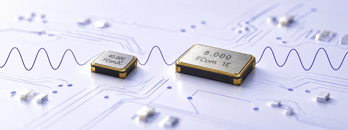
No. The resonator waveform and the module’s output waveform differ. The output stage may provide logic, differential or clipped-sine signaling; use its datasheet.
Does XTAL mean the same thing as XO?
Usually XTAL identifies a resonator and XO identifies an oscillator. Confirm the meaning from the component’s electrical functions.
Technical references
- Microchip, AN826: Crystal Oscillator Basics and Crystal Selection, DS00826A, 2002. PDF.
- STMicroelectronics, AN2867: Guidelines for oscillator design, Rev 24, February 2026. PDF.
- NDK, Crystal oscillator terminology.
- Microchip, ANTC207: Quartz Crystals and Microchip ICs, DS00002187A, 2016. PDF.
- Texas Instruments, SNLA290: Selection and specification of crystals for Ethernet PHYs, February 2019. PDF; device-specific requirements apply.
- Analog Devices, MT-008: Converting Oscillator Phase Noise to Time Jitter. PDF.