VCXO · Communication Synchronization · PLL Design
A communication clock must often follow an external reference while limiting timing noise. A voltage-controlled crystal oscillator (VCXO) provides the adjustable clock source within that synchronization loop. Successful selection depends on usable tuning margin, loop dynamics and measured noise—not simply nominal frequency or a typical jitter figure.
FCom Fuji Crystal · Technical Guide
How a VCXO Works
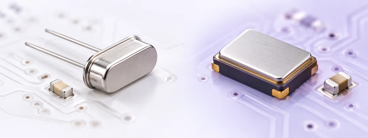
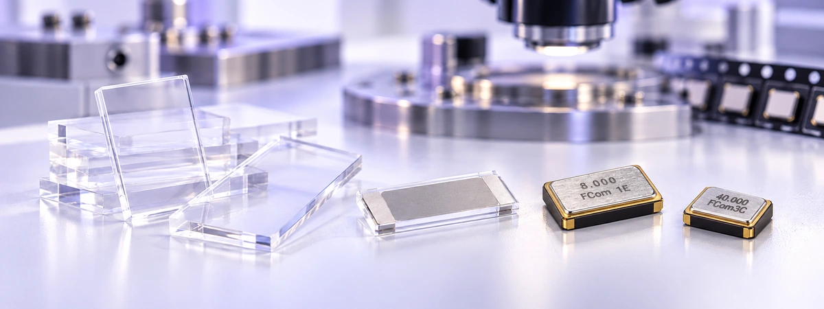
A quartz VCXO combines a crystal resonator, sustaining electronics and a voltage-controlled tuning function. In a conventional design, a variable capacitance changes the resonator’s effective loading and slightly shifts its oscillation frequency. Synthesized architectures can implement voltage control differently; the applicable datasheet defines the behavior. [1]
Voltage control does not itself provide temperature compensation. A VCXO and a temperature-compensated VCXO, often called a VCTCXO, serve different stability requirements. Likewise, “programmable” does not automatically mean that the user can change frequency through a digital interface: confirm how the selected device is configured.
Reference and Adjustable-Source Roles in a PLL
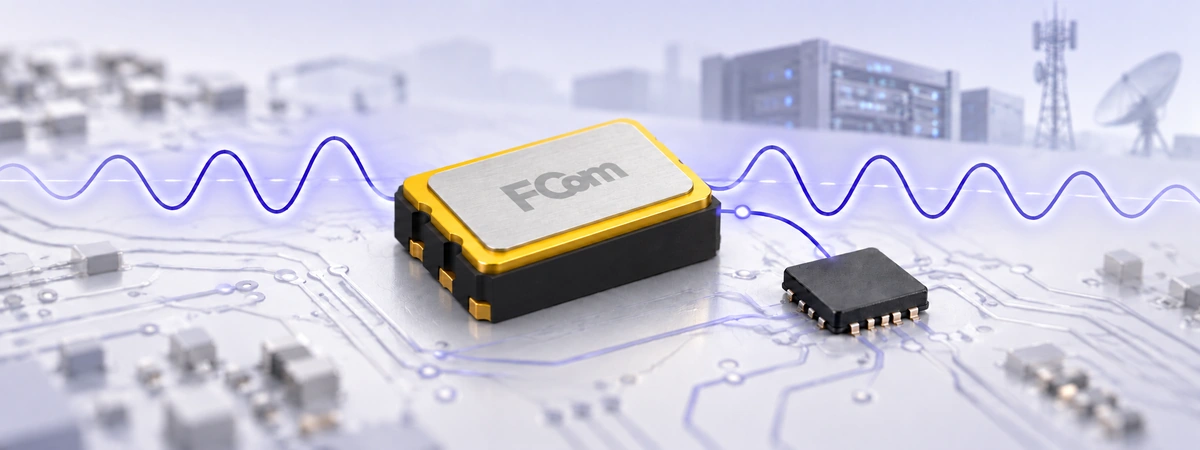
In a VCXO-based synchronization PLL, the reference establishes the timing relationship to be followed. The VCXO produces the local adjustable clock. These are separate roles, even when both signals originate from crystal-based devices.
- Compare: a phase-frequency detector compares the reference with feedback derived from the VCXO.
- Filter: the loop filter converts the detector or charge-pump output into a control voltage and shapes the loop response.
- Adjust: the VCXO changes frequency according to that voltage.
- Feed back: the output returns through the feedback path, with division where required.
For an integer-ratio loop with reference divider R and feedback divider N, the locked relationship is:
fout = (N / R) × fref
The selected VCXO’s nominal frequency must already be close enough to that target for its tuning range to reach it. The divider ratio does not make a narrow-range VCXO into a wideband oscillator. [2]
This architecture supports recovered-clock tracking, network timing distribution and synchronized equipment clocks. Clock recovery still requires suitable detection and control circuitry; a VCXO alone does not extract a clock from a data stream.
Pull Range, APR and Tuning Gain
Pull range describes frequency adjustment across a stated control-voltage interval. APR describes the guaranteed correction range remaining after the specified frequency-error budget is allowed for. That budget can include initial tolerance, temperature, supply, load and aging. Check which effects and service-life interval the supplier includes. [3]
Illustrative budget—not FCom product data: assume a symmetric tuning capability of ±120 ppm, maintained over the specified conditions, and a total center-frequency error of ±45 ppm. The remaining symmetric correction margin is ±75 ppm.
If the reference requires ±50 ppm tracking, this leaves 25 ppm of margin on each side. Use one-sided magnitudes consistently: the 240 ppm peak-to-peak span cannot be substituted for 120 ppm in this subtraction.
This estimate does not replace a guaranteed APR specification. Avoid subtracting temperature or aging twice when they are already included, and check the upper and lower limits separately if tuning is asymmetric. Sufficient APR is necessary for tracking, but does not alone guarantee PLL acquisition or stability.
Tuning gain and control-voltage headroom
Tuning gain Kv is the local frequency change per volt, expressed in Hz/V or ppm/V. For Kv in ppm/V:
Δf ≈ f0 × Kv × ΔVc × 10−6
Include gain variation, control polarity and modulation bandwidth in the loop model. Keep the required control voltage inside both the VCXO’s specified interval and the driver’s output swing. A typical average Kv does not describe every operating point. [1] [3]
Loop Bandwidth Determines Jitter-Cleaning Behavior
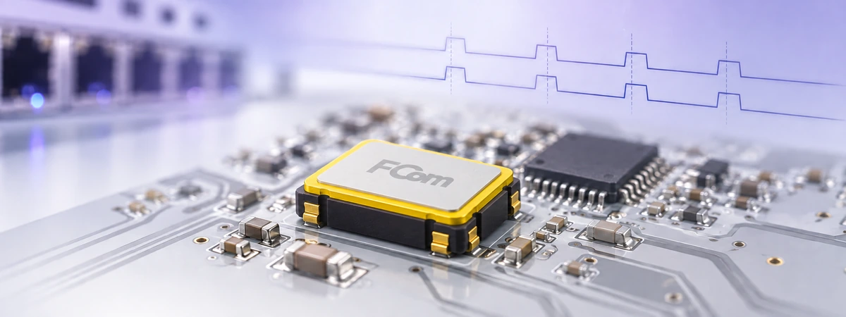
A PLL redistributes noise rather than removing all of it. Inside the loop bandwidth, reference and PLL circuitry noise contribute strongly while the VCXO’s own phase fluctuations are suppressed. Outside it, reference-noise transfer is attenuated and the VCXO’s free-running noise becomes more important. Other circuit noise can also contribute. [4]
A narrower loop can reject more reference noise, but responds more slowly. Choose bandwidth using reference and VCXO phase-noise curves, settling requirements and loop stability. Include noise coupled into Vc, because tuning gain converts it into frequency modulation. Added control-pin filtering must be included in the loop model.
Compare RMS phase jitter using the same integration band, output frequency, operating mode, supply and load conditions. A 12 kHz–20 MHz jitter figure does not describe low-frequency wander or prove compliance with a complete communications timing requirement.
FCom FVC Series: Select by Package and Tuning Specification
FVC-3P-LJ, FVC-5P-LJ and FVC-7P-LJ provide CMOS FASTVCXO options in three package sizes. The catalogue frequency range identifies supported nominal outputs; it is not the analog tuning span of an individual ordered device.
| Series | Package (mm) | Frequency / output | Pull-range distinction | Technical file |
|---|---|---|---|---|
| FVC-3P-LJ | 3.2 × 2.5 | 10–250 MHz / CMOS | Frequency pulling range is listed separately from APR. Request guaranteed APR for the selected configuration. | FVC-3P-LJ PDF |
| FVC-5P-LJ | 5.0 × 3.2 | 10–250 MHz / CMOS | Minimum APR: ±50 ppm in the catalogue table. | FVC-5P-LJ PDF |
| FVC-7P-LJ | 7.0 × 5.0 | 10–250 MHz / CMOS | Minimum APR: ±50 ppm in the catalogue table. | FVC-7P-LJ PDF |
For all three series, the catalogue lists RMS phase jitter over 12 kHz–20 MHz: 0.6 ps typical / 1.2 ps maximum in integer mode, and 0.8 ps typical / 1.5 ps maximum in fractional mode. The electrical tables state an ambient test temperature of 25 ±5 °C. Select the operating mode and confirm the applicable limits for the ordered frequency.
For a 5032 design, FVC-5P-LJ is the corresponding named series to evaluate. Specify the complete configuration and verify pinout, voltage limits, temperature grade and loading before approving a replacement. Confirm delivery against the quotation for that configuration.
Integration and Validation
- Build the frequency budget: document reference deviation, guaranteed APR, aging interval and control-voltage margin.
- Model the loop: check Kv limits, phase margin, peaking, settling and acquisition behavior.
- Protect the control node: keep Vc routing away from switching nodes and fast clock traces; use local supply decoupling.
- Verify the receiver: confirm CMOS voltage thresholds, loading, edge rates and enable behavior.
- Test the system: measure lock behavior and output jitter across operating conditions, including reference loss and recovery.
Frequently Asked Questions
Is a VCXO a complete PLL?
No. It is the adjustable oscillator. A synchronization PLL also needs phase comparison, a loop filter and a feedback path.
Can a 10–250 MHz VCXO sweep that entire range through Vc?
No. That catalogue range describes nominal frequency coverage. Analog voltage control makes a much smaller correction around the configured frequency.
Does ±150 ppm pull range guarantee ±150 ppm APR?
No. APR accounts for the specified frequency-error allowances. A pull-range entry must not be relabeled as APR.
Does a VCXO guarantee holdover after reference loss?
No. Holdover depends on oscillator drift and the system’s control-voltage retention or prediction strategy. Specify the allowable error and holdover duration separately.
Discuss Your VCXO and PLL Requirements
Send FCom your target frequency, package, supply, output load, temperature range, required APR, control-voltage swing and jitter integration band. Include the PLL architecture and loop bandwidth where available. Contact FCom@fujicrystal.com for model-specific documentation and configuration review.
Technical References
FCom model-specific catalogue PDFs are linked in the selection table above.