FCom Fuji Crystal · Technical Guide
Selecting a quartz timing component requires more than choosing a frequency. The circuit must also meet its frequency-error budget, noise limits, startup requirements and electrical interface specifications. This guide explains the parameters that distinguish a suitable crystal or oscillator from a part that merely has the right nominal frequency.
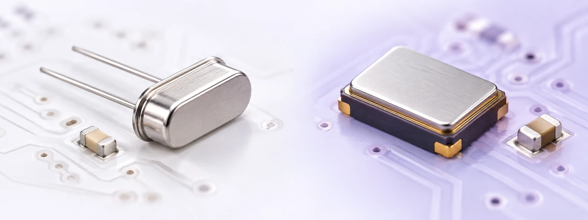
Start with the device type: an XTAL is a passive quartz resonator that needs an active oscillator circuit. A packaged crystal oscillator contains the resonator and active circuitry, accepts a power supply and delivers a specified output signal. Their selection criteria overlap, but they are not interchangeable components.
How quartz oscillation works
Quartz couples electrical excitation to mechanical vibration through piezoelectricity. Its resonant response supplies frequency selectivity, while an amplifier replenishes energy lost in the resonator and circuit.
The electrical model contains a series motional resistance, inductance and capacitance in parallel with a shunt capacitance. In a Pierce circuit, the crystal, amplifier and load network operate together. Startup requires adequate small-signal gain or negative-resistance margin; a steady-state loop condition alone does not guarantee reliable startup. [1]
XTAL, XO, TCXO, VCXO and OCXO
| Type | Function | Selection priority |
|---|---|---|
| XTAL | Passive quartz resonator. | Compatibility with the host oscillator circuit. |
| XO | Packaged oscillator providing a clock output. | Frequency, stability, supply, output and noise. |
| TCXO | Electronically compensates temperature-related frequency changes. | Specified temperature stability and operating conditions. |
| VCXO | Allows frequency adjustment through a control voltage. | Pull range, control characteristic and noise. |
| OCXO | Controls the resonator’s temperature with an oven. | Warm-up, power, stability and aging. |
These labels describe functions, not guaranteed performance grades. Temperature compensation and voltage control can coexist in a VCTCXO. Compare the actual specifications rather than assuming one family always has lower jitter or slower aging.
Frequency, tolerance and stability
Nominal frequency and frequency planning
Select the frequency required by the receiving IC and clock architecture. A 32.768 kHz timebase equals 215 Hz and can be divided to 1 Hz. Other familiar references include 10 MHz in instrumentation and frequencies such as 19.2, 25, 26 or 38.4 MHz in digital and radio systems. These are examples, not universal interface requirements.
Read the complete error budget
- Initial tolerance: frequency offset under stated reference conditions.
- Temperature stability: frequency variation over a defined temperature range and reference convention.
- Supply and load sensitivity: frequency changes as voltage or output loading varies.
- Aging: gradual frequency change over a stated interval and environment.
A quoted “±20 ppm” is incomplete without its conditions. Determine whether it covers temperature alone or a combined set of effects. Add separate worst-case terms only when they are not already included; do not count the same contribution twice.
Frequency error (Hz) = nominal frequency (Hz) × error (ppm) / 1,000,000
Example: ±20 ppm at 25 MHz corresponds to ±500 Hz. A constant 10 ppm error accumulates about 0.864 seconds in 24 hours without correction. These are illustrative calculations, not FCom product measurements.
Phase noise, jitter and Allan deviation
Phase noise describes phase fluctuations in the frequency domain, commonly as single-sideband noise in dBc/Hz at specified offsets from the carrier. Jitter describes timing variation. Period jitter, cycle-to-cycle jitter and integrated phase jitter are different measurements.
Compare RMS phase-jitter values only with their integration limits, carrier frequency and measurement conditions. A result integrated from 12 kHz to 20 MHz cannot be compared directly with one using a different offset band. Analog Devices explains the phase-noise integration and conversion to time jitter in MT-008. [2]
For precision frequency analysis, Allan deviation describes fractional-frequency fluctuations versus averaging time, τ. It is distinct from a datasheet’s temperature-stability limit; the averaging time and analysis method must accompany the value. [5]
Load capacitance, ESR and drive level
For a load-rated parallel-resonant crystal, the specified frequency assumes a stated load capacitance, CL. A common first approximation for a Pierce network is:
CL ≈ (CA × CB) / (CA + CB) + Cstray
CA and CB represent the two load capacitors; Cstray represents the effective parasitic contribution in this simplified model. With two 18 pF capacitors and 3 pF effective stray capacitance, the estimated load is 12 pF. Validate it on the actual board. Frequency pulling also depends on the crystal’s motional and shunt capacitances, so load-capacitance percentage alone cannot determine a ppm shift. [3]
ESR, specified in ohms, represents resonator loss and affects startup margin. Drive level, usually specified in microwatts, is power dissipated in the crystal. Verify both against the host circuit and crystal ratings. Fundamental and overtone crystals also require compatible oscillator circuits. [1]
Output formats and interfaces
| Output | Interface | Check before connection |
|---|---|---|
| CMOS / LVCMOS / HCMOS | Single-ended logic. | Supply, logic thresholds, capacitive load and edge rates. |
| LVDS | Differential signaling. | Differential swing, common-mode range and termination; often 100 Ω at the receiver. |
| LVPECL | Differential signaling with specific bias requirements. | DC bias, termination and any AC-coupling network. |
| HCSL / LP-HCSL | Differential clock interfaces. | Driver architecture and prescribed termination. |
| Sine / clipped sine | Analog waveform. | Amplitude, bias, load impedance and receiver sensitivity. |
“TTL-compatible” describes compatibility with defined logic thresholds; it is not a substitute for checking voltage limits. Differential outputs are not interchangeable simply because both have two pins. Follow the oscillator and receiver recommendations for termination and coupling, accounting for any internal termination. TI provides practical interface examples. [4]
Selection and board validation
- Define the requirement: frequency, temperature range, lifetime error budget, jitter or phase-noise limits, and receiver interface.
- Check electrical details: supply tolerance, current, output load, duty cycle, rise/fall times, pinout and package.
- Check timing behavior: power-on startup, enable delay and disabled-output state. OCXO warm-up to specified accuracy is separate from first output activity.
- Validate the board: test startup across voltage and temperature, use recommended decoupling and routing, and measure the clock at its receiver.
Use a suitable reference for frequency measurements and low-loading probes around crystal nodes. For RF or high-speed conversion, inspect noise at the relevant offsets and bandwidth. For low-power duty-cycled systems, include startup energy and recovery time in the power budget.
Frequently asked questions
Can a crystal replace a powered oscillator module?
No. A passive crystal requires an active oscillator loop. A module requires power and presents a specified output interface; use the connection method supported by the receiving IC.
Does tighter ppm stability guarantee lower jitter?
No. Frequency-error limits and timing noise describe different behavior. Specify both when the application requires them.
Should each load capacitor equal the crystal’s CL?
No. The effective load depends on both capacitors and circuit parasitics. Use the appropriate network model and verify frequency and startup on the PCB.
Does output enable always stop oscillation?
No. Some controls disable only the output buffer, while standby may stop internal circuitry. Check current consumption, output state and restart timing in the datasheet.
Need help defining a timing component? Send FCom your target frequency, device type, supply, output format, temperature range, error budget, noise requirements and package constraints at FCom@fujicrystal.com. For a passive crystal, include the host IC, load capacitance, ESR limit and drive requirements.
Technical references
- STMicroelectronics. AN2867: Guidelines for oscillator design on STM8AF/AL/S and STM32 MCUs/MPUs. PDF.
- Analog Devices. MT-008: Converting Oscillator Phase Noise to Time Jitter. PDF.
- Seiko Epson. Oscillator Circuit Evaluation Method (1): Frequency Matching. Technical notes, PDF.
- Texas Instruments. SNAA377: Termination Guidelines for Differential and Single-Ended Signals. PDF.
- Riley, W. J. Handbook of Frequency Stability Analysis. NIST Special Publication 1065, 2008.