FCom Fuji Crystal · Technical Guide
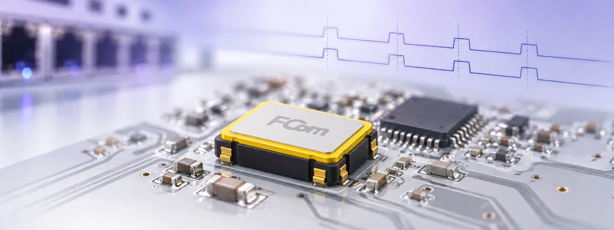
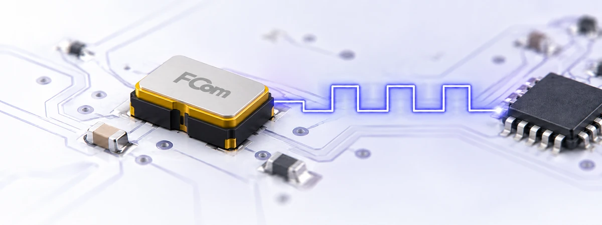
A CMOS crystal oscillator provides a clock signal for a compatible digital input. Selection starts with the receiving IC: its required frequency, voltage thresholds, waveform limits and timing budget determine which oscillator configuration will work.
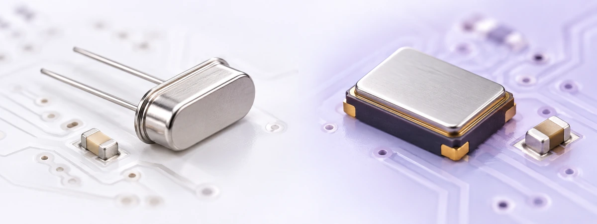
What is a CMOS crystal oscillator? It is a powered timing component containing a quartz resonator, sustaining circuitry and a CMOS output stage. It supplies a periodic logic clock after startup. A passive quartz crystal relies on an oscillator circuit outside the crystal package.
How a CMOS crystal oscillator works
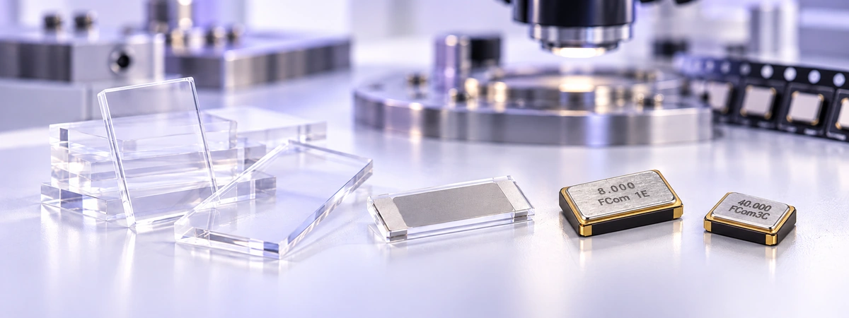
Quartz’s piezoelectric behavior links electrical excitation to mechanical vibration. In the oscillator feedback loop, the crystal selects a resonance while the active circuitry replaces energy lost in each cycle. An output stage then drives the external clock input.
Some designs include frequency synthesis or division. Their clock output therefore need not equal the quartz resonator’s mechanical frequency. Check the architecture and functions of the selected part rather than inferring them from its output frequency.
CMOS means complementary metal-oxide-semiconductor; LVCMOS denotes low-voltage CMOS signaling. In a timing datasheet these labels describe an output interface, while XO, TCXO and VCXO describe oscillator functions.
| Term | What it identifies | What to verify |
|---|---|---|
| Quartz crystal | Passive resonator | Compatible host oscillator circuit, load and drive level |
| Standard XO / SPXO | Packaged oscillator without temperature compensation or oven control | Its specified frequency-error limits |
| TCXO / VCTCXO | Temperature compensation; VCTCXO also permits voltage-controlled adjustment | Stability definition, output and any usable tuning range |
| VCXO | Voltage-controlled frequency adjustment | Pull range and control-input conditions |
| CMOS / LVCMOS | Single-ended logic signaling referenced to ground | Guaranteed logic levels, load and edge rates |
| LVDS / LVPECL | Differential signaling interfaces | Receiver compatibility and interface-specific termination |
A TCXO or VCXO may have a CMOS output. The CMOS label alone establishes neither temperature compensation nor a particular jitter performance.
Benefits and typical applications
A packaged oscillator removes the need to build its quartz sustaining circuit on the PCB. It can supply MCU, FPGA, communications, measurement and industrial-control clock inputs when their interfaces are compatible. Compact packaging can simplify placement, but low current, fast startup, low phase noise and environmental qualification remain properties of the ordered device.
A practical CMOS oscillator selection checklist
- Frequency and accuracy: confirm the required clock rate and which initial, temperature, supply, load and aging terms are included in the stated frequency limit.
- Supply and output levels: compare guaranteed output levels with receiver thresholds across the applicable voltage, temperature and loading conditions.
- Load and waveform: include receiver input capacitance, interconnect and parasitics. Retain the datasheet’s load and threshold definitions for duty cycle and rise/fall time.
- Jitter: specify the receiver’s required metric, carrier frequency, integration band where relevant, and RMS or peak-to-peak basis.
- Power and control: check loaded current, startup, output-enable or standby behavior, and the time to a valid clock.
- Physical and environmental fit: verify dimensions, pad pattern, pin functions, operating temperature, assembly profile and any required qualification documentation.
Match output levels to the receiver
Compare the oscillator’s minimum guaranteed high level VOH(min) with the receiver’s VIH(min), and its maximum low level VOL(max) with VIL(max). Use the specified supply, temperature and output-current or loading conditions, allowing positive DC noise margins:
A 3.3 V oscillator may drive a 1.8 V input only when that input explicitly permits the applied voltage and sequencing conditions. Otherwise, use a compatible oscillator supply/output or a suitable clock-level translator. Include the translator’s delay, duty-cycle effects and added jitter in the design. TI SCEA035A (PDF) explains the underlying logic-level compatibility checks.
Frequency accuracy and jitter answer different questions
Frequency error is the departure of the clock rate from nominal. Jitter describes edge-timing variation using a specified measurement method. A low-jitter output can still have a frequency offset, and temperature compensation does not replace a jitter requirement.
Compare initial tolerance, temperature stability, supply/load effects and aging on consistent terms. Avoid adding a term again when it is already included in an overall limit. Aging must retain its stated interval, reference conditions and Typ./Max. basis.
Period jitter, cycle-to-cycle jitter and integrated phase jitter are not interchangeable. For phase noise, retain the carrier and offset frequencies; for integrated phase jitter, retain the integration band and any filtering. See SiTime AN10007 for the measurement definitions.
Calculated example: 25 MHz at ±20 ppm
Frequency deviation = nominal frequency × ppm / 1,000,000. Thus, 25,000,000 × 20 / 1,000,000 = 500 Hz, giving a ±500 Hz deviation.
A constant 20 ppm offset in an uncorrected time counter produces a time-error magnitude of 86,400 × 20 / 1,000,000 = 1.728 seconds per day. These calculations are illustrative, not a FCom rating or measured holdover result; changing conditions and system correction affect actual time error.
Output load, power and control functions
For a full-swing capacitive clock load charged once per output cycle, first-order estimates are:
For example, assuming 15 pF, 3.3 V and 25 MHz gives approximately 1.24 mA of load-related supply current and 4.08 mW of load-related power. Internal oscillator consumption and other losses are additional. If a datasheet current already includes the same output load, do not add this estimate again.
DC supply tolerance does not define acceptable AC ripple. Check the relevant noise-sensitivity information and decoupling guidance, then measure the real rail and receiving waveform.
| Event / function | What to confirm |
|---|---|
| Power-on startup | Supply-ramp conditions, startup definition and time to the required output validity or frequency accuracy |
| Output enable (OE) | Whether only the buffer is disabled; output state, control thresholds, current and enable/disable timing |
| Standby / shutdown | Which circuits stop; standby current, resume time and the output state during recovery |
OE and standby names do not establish a universal recovery time or pin behavior. Do not assume that a disabled output means the oscillator core has stopped, or that re-enabling it is equivalent to a fresh power-on.
PCB integration and board validation
- Decoupling: follow the part’s supply guidance and minimize the connection loop between the supply, capacitor and ground.
- Routing: provide a continuous return path and control stubs and fanout. Evaluate transmission-line behavior from edge speed and propagation delay, not clock frequency alone.
- Termination: where source termination is needed, use the actual driver and interconnect characteristics. Confirm it with an appropriate model or receiver waveform rather than a universal resistor value.
- Measurement: inspect the signal at the receiving pin using a suitable probe. Account for its loading when judging amplitude, ringing, overshoot and edge rate.
- Operation: set the host’s specified external-clock mode. Test power sequencing, enable/standby transitions, supply and temperature corners, and representative switching activity.
SiTime AN10002 discusses single-ended termination and multiple-load layouts. Its device-specific driver values are not FCom specifications. Record the final ordering code, load, PCB revision, instrument settings and acceptance limits with the board results.
CMOS crystal oscillator FAQ
Can it directly replace a passive crystal?
No. A powered oscillator needs supply connections and a compatible external-clock input. Confirm the host’s allowed input pin, signal levels and configuration before changing the architecture.
Does it need the two external crystal load capacitors?
Normally, its resonator network is internal. Do not copy the two-capacitor network from a passive-crystal circuit onto the oscillator output. Follow the selected device’s decoupling and output-interface requirements.
Can any 3.3 V CMOS clock drive a 1.8 V receiver?
No. Both guaranteed logic levels and the receiver’s permitted input voltage must be satisfied, including relevant power-off conditions. Use a compatible output or clock translator when needed.
Does OE always save as much power as standby?
No. OE may leave the core running while disabling the output. Standby may stop more circuitry and require a longer recovery. Check the specified states, current and timing for the ordered option.
When should a TCXO be considered?
When the standard XO’s documented frequency limits cannot meet the temperature-dependent system budget. Its waveform, jitter, supply, power and startup must also fit the receiver.
FCom product and design resources
- Crystal oscillator families — review the selected CMOS/LVCMOS configuration in its individual datasheet.
- Oscillator Selection Guide — compare oscillator functions and selection requirements.
- Crystal Oscillators Product Selection Guide (PDF) — portfolio overview covering several output and performance groups.
- Industrial Timing Guide — apply clock selection to controller, interface, radio and RTC roles.
Discuss your clock requirements with FCom
Share the receiving IC, frequency, supply, output format, load, stability and jitter requirements, temperature range and package limits. Include the schematic or interconnect details when interface compatibility or waveform quality is the main concern.
Technical references
- Epson, Basic Knowledge of Crystal Unit and Crystal Oscillators: quartz behavior and oscillator functions.
- Texas Instruments, Selecting the Right Level-Translation Solution, SCEA035A, June 2004: logic-level compatibility.
- SiTime, AN10002: Termination Recommendations for Single-ended Oscillator Driving Single or Multiple Loads.
- SiTime, Timing Terminology Glossary and AN10007: Clock Jitter Definitions and Measurement Methods.
- SiTime, Oscillator FAQs: capacitive-load current, supply noise and OE/standby examples. Device-specific figures do not establish FCom ratings.