FCom / News & Events
FCO-6LH · FCO-2LH · High-fundamental quartz technology
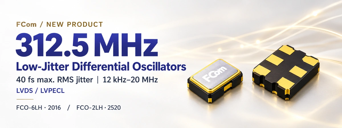
FCom introduces the FCO-6LH and FCO-2LH 312.5 MHz differential crystal oscillators for optical transceivers and high-speed networking designs. The two series combine high-fundamental quartz technology with LVDS or LVPECL output, providing a compact reference-clock solution for compatible optical DSP, SerDes and clock-synthesis inputs.
The featured 312.5 MHz configurations offer 40 fs maximum RMS phase jitter, integrated from 12 kHz to 20 MHz under the applicable datasheet test conditions. Designers can select a 2016 or 2520 package to suit board-space and layout requirements. For projects targeting ±20 ppm frequency stability or operation from −40 to +105°C, FCom can review the required configuration and confirm the part-specific specification.
Two Package Options for 312.5 MHz Reference Clocks
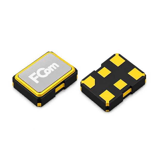
FCO-6LH
2016 · nominal 2.0 × 1.6 mm · six-pad SMD
The smaller package option supports space-constrained optical modules and compact networking boards requiring a 312.5 MHz LVDS or LVPECL reference.
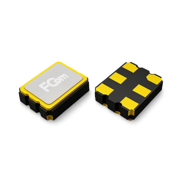
FCO-2LH
2520 · nominal 2.5 × 2.0 mm · six-pad SMD
The 2520 option brings the same high-fundamental quartz technology to designs using a larger package footprint, with 312.5 MHz LVDS or LVPECL configurations.
2016 and 2520 identify nominal package classes. Refer to each product’s mechanical drawing for the controlled dimensions and PCB land pattern.
Low Jitter with LVDS and LVPECL Output Options
The two series provide a common performance platform across different package sizes. Output interface, supply voltage and temperature grade are selected to match the receiving device and the operating environment.
| Parameter | Configuration Highlights |
|---|---|
| Nominal output frequency | 312.5 MHz, fixed-frequency configuration |
| RMS phase jitter | 40 fs max.; integration bandwidth: 12 kHz–20 MHz |
| Frequency-stability requirement | ±20 ppm target; confirm the applicable conditions and aging allowance in the agreed specification |
| Output interface | LVDS or LVPECL, selected at ordering |
| Nominal supply options |
LVDS: 1.8 V / 2.5 V / 3.3 V LVPECL: 2.5 V / 3.3 V |
| Operating-temperature requirement | −40 to +85°C or −40 to +105°C target range; confirm the grade for the selected configuration |
The 40 fs maximum jitter figure applies under the published datasheet test conditions; the LVDS jitter note specifies measurement at 3.3 V. Confirm the selected output and supply voltage before design-in. Frequency-stability limits, operating-temperature range and aging allowance are defined in the agreed part-specific specification.
For guidance on interpreting the stated integration band and comparing clock-noise measurements, see phase noise and RMS jitter explained.
LVDS vs LVPECL for Optical DSP and SerDes Reference Clocks
The receiving optical DSP or SerDes defines the required reference frequency, differential swing, common-mode range and allowable input voltage. Select LVDS or LVPECL against those limits, then verify the coupling, bias and termination network specified for the oscillator and receiver. Review the complete clock path, including the oscillator, buffers, clock synthesizers and routing, against the receiver’s jitter and phase-noise requirements. Compare total clock-path power, including output-stage current, termination and any required translation. Our LVDS and LVPECL reference-clock interface guide explains these checks for optical DSP and SerDes designs; confirm the selected device configuration before layout.
High-Fundamental Quartz Technology
FCO-6LH and FCO-2LH use a quartz resonator operating in its fundamental mode at high frequency. This architecture supports low source phase noise and low integrated jitter, giving designers two package options based on the same underlying quartz technology.
For optical DSP and SerDes reference inputs, oscillator noise forms part of the complete clock budget. Evaluation should consider the receiver’s phase-noise mask, jitter integration bandwidth and clock-transfer characteristics, together with supply noise and any clock-distribution stages.
Reference Clocks for Optical Modules and High-Speed Networking
The series support evaluation in 800G and 1.6T optical transceiver architectures that specify a 312.5 MHz differential reference input . Compact packaging and low source jitter address key requirements in optical DSP and PAM4 SerDes clock paths, while the operating-temperature grade should be selected for the actual temperature at the oscillator location.
Additional design opportunities include compatible Ethernet switch ASICs, FPGA transceivers, clock-synthesis circuits and evaluation platforms requiring a 312.5 MHz reference. Selection includes review of differential swing, common-mode voltage, coupling and termination, as well as the frequency and jitter budget.
Explore FCom’s RF & High-Speed Digital application solutions for related optical-module, networking and SerDes design support.
Need 285 MHz or 625 MHz?
285 MHz is also listed in the FCO-6LH and FCO-2LH datasheets. For projects requiring a 625 MHz differential oscillator, contact FCom to review the required package, output interface and performance targets. Our team can confirm the appropriate configuration, applicable specifications and availability for your design.
Product Information and Design-In Support
Review the FCO-6LH and FCO-2LH product pages for datasheets and configuration details. For selection guidance, quotation or sample requests, send FCom your target frequency, preferred package, output interface, supply voltage, operating-temperature range and receiver part number, together with the required jitter bandwidth and sample quantity.