Clock Interfaces · Technical Guide
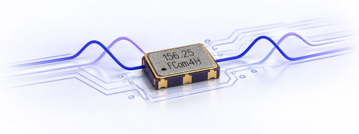
LVDS stands for Low-Voltage Differential Signaling. It carries information as a small voltage difference between two conductors and is used for both data transmission and clock distribution.
FCom Fuji Crystal · Technical Guide
How LVDS works
The receiver responds to the difference between its positive and negative inputs. A typical driver steers approximately 3.5 mA through a 100 Ω termination, producing a differential voltage magnitude of about 350 mV. Reversing the current reverses the signal polarity. [1]
Illustrative calculation:
Vdiff = V+ − V−
|Vdiff| = I × R = 3.5 mA × 100 Ω = 350 mV
In this example, the differential signal alternates between approximately +350 mV and −350 mV, giving about 700 mV peak-to-peak. These are illustrative nominal values, not FCom product measurements.
The common-mode voltage is the average of the two conductor voltages. Conventional LVDS outputs commonly center around 1.2 V, but actual output levels and receiver limits must be checked in the relevant datasheets. “Low voltage” describes the signal swing; it does not specify the device supply voltage. [3]
Benefits and limits
Small signal swings and balanced current paths can reduce switching noise and radiated emissions. A differential receiver can reject noise that reaches both conductors similarly, provided its common-mode operating limits are respected. [1]
These benefits depend on the complete interconnect. Unbalanced routing, impedance discontinuities and excessive loading can degrade the signal. LVDS does not specify a communication protocol, connector, universal cable length or guaranteed system data rate.
Likewise, the output format alone does not guarantee low jitter, frequency stability, an extended temperature range or automotive qualification. Those are separate device specifications. Total power also includes the oscillator circuitry and receiver, not just the termination.
LVDS, LVCMOS and LVPECL
Choose the interface required by the receiving device. Different output families have different voltage levels and loading requirements; matching the clock frequency alone is insufficient. [3]
| Interface | Signal format | Design consideration |
|---|---|---|
| LVDS | Differential, with a small voltage swing. | Usually uses a 100 Ω differential receiver termination; check for internal termination. |
| LVCMOS | Usually single-ended and referenced to ground. | Match input voltage thresholds and capacitive loading; assess transmission-line effects. |
| LVPECL | Differential, typically with a larger swing than LVDS. | Requires a suitable bias and termination network to maintain output current. |
LVDS often offers simpler termination and lower interface power than LVPECL. However, neither family is always the lowest-jitter choice: driver performance, receiver slew rate and board implementation matter. [5]
Termination and PCB layout
DC-coupled connections
For a conventional point-to-point LVDS connection, place the 100 Ω termination across the two inputs close to the receiver. First check whether the receiver already integrates this resistor. Adding another 100 Ω in parallel creates a 50 Ω load and changes the signal amplitude. [4]
AC-coupled connections
AC coupling blocks the driver’s DC level. The receiver must then establish an appropriate input bias internally or through an external network. Preserve the driver’s required current path and select coupling capacitors for the operating frequency and startup behavior; follow both device datasheets. [4]
Routing priorities
- Design the pair for the specified differential impedance, commonly 100 Ω.
- Keep routing balanced and control intra-pair skew.
- Maintain a continuous reference plane and minimize stubs and unnecessary vias.
- Place supply decoupling close to the device and separate clocks from noisy switching nodes.
Review the complete path, including connectors and receiver loading. Verify signal quality at the receiver under the intended operating conditions. [2]
Selecting an LVDS oscillator
LVDS clocks are used in communications equipment, FPGA-based systems and instrumentation where compatible differential inputs are available. Selection starts with the receiver requirements and the system timing budget.
- Frequency: Specify the required output frequency and permitted deviation over the relevant operating conditions.
- Electrical compatibility: Confirm supply voltage, differential amplitude, common-mode range, termination and coupling.
- Timing performance: Define duty cycle and the required jitter metric. For integrated RMS phase jitter, state the offset-frequency integration range.
- Environment: Confirm operating temperature, aging requirements and any application-specific qualification.
- Integration: Check package, pin assignment, enable behavior, startup time and power budget.
A ppm frequency specification and a jitter specification describe different aspects of timing. Compare candidate oscillators using matching definitions and test conditions.
Frequently asked questions
Is LVDS a communication protocol?
No. It defines electrical signaling characteristics. Framing, encoding and the meaning of transmitted data are determined elsewhere in the system. [1]
Can an LVDS output connect directly to LVCMOS?
Generally, no. Use a suitable receiver or translator unless the destination explicitly supports the source levels. Check differential amplitude, bias and input limits before connecting different families. [3]
Can one LVDS oscillator drive several receivers?
Do not assume it can drive several independently terminated branches. Additional loads and stubs change the interconnect. A suitable clock fanout buffer provides separate outputs when multiple clock destinations are required. [5]
Does LVDS guarantee better clock accuracy?
No. Frequency accuracy depends on the oscillator design and its specified conditions. LVDS describes how the clock is delivered, not how accurately its frequency is generated.
Discuss your clock requirements
For an FCom oscillator inquiry, send your target frequency, supply voltage, receiver part number, package, temperature range and jitter requirements to FCom@fujicrystal.com. Include the planned termination and coupling circuit to support compatibility review.
Technical references
- Texas Instruments: An Overview of LVDS Technology (PDF) .
- Texas Instruments: LVDS Owner’s Manual, Fourth Edition (PDF) .
- Texas Instruments: Interfacing Between LVPECL, VML, CML and LVDS Levels (PDF) .
- Texas Instruments: LMK04906 Datasheet (PDF) , Section 9.1.3: termination and clock outputs.
- Analog Devices: AD9522-2 Product FAQ , clock fanout, termination and output comparisons.
Reference circuits illustrate interface principles. Use the datasheets for your selected oscillator and receiver to determine the final implementation.