
FSF-5050 Series · SAW Bandpass Filter
499 & 499.25 MHz SAW Bandpass Filters
FSF-5050-499M · FSF-5050-499M25
Two frequency options for RF/IF signal selection in UHF receiver and measurement front ends, in a 5.0 × 5.0 mm SMD package.
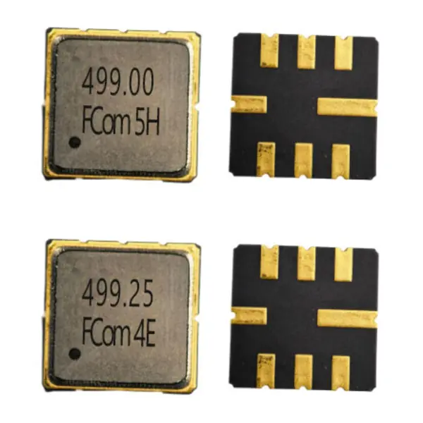
Left: marked top surface. Right: pad side. Photos do not define pin orientation.
Model Selection
Choose by Signal Band and Test Conditions
The two models share a package but differ in specified passband, insertion loss, ripple definition, test terminations and operating temperature. A 0.25 MHz difference in center frequency does not make them interchangeable.
FSF-5050-499M
499 MHz
Center frequency (Typ.)
- Specified passband
- 494–504 MHz
- Insertion loss over 494–504 MHz
- 2.0 dB typ. / 4.0 dB max.
- Source / load test terminations
- 50 Ω / 50 Ω
- Operating temperature
- −40 to +85 °C
FSF-5050-499M25
499.25 MHz
Center frequency (Typ.)
- Ripple test band
- 498.75–499.75 MHz
- Insertion loss at 499.25 MHz only
- 2.2 dB typ. / 5.0 dB max.
- Source / load test terminations
- 75 Ω / 75 Ω
- Operating temperature
- −20 to +70 °C
A 0.25 MHz difference in center frequency does not make these models interchangeable. Their loss specifications cover different frequency conditions, their ripple definitions must be preserved, and their test terminations differ.
Electrical Specifications
Keep Each Limit with Its Frequency Condition
“—” means a value is not specified, not zero. Typical values are for design guidance. Neither model has a specified 3 dB bandwidth.
FSF-5050-499M
Scroll horizontally to view all columns.
| Parameter | Min. | Typ. | Max. | Unit | Definition / condition |
|---|---|---|---|---|---|
| Center frequency | — | 499.0 | — | MHz | FCom Typ. column |
| Specified passband | — | — | — | MHz | 494–504 MHz; insertion-loss and ripple interval |
| Insertion loss | — | 2.0 | 4.0 | dB | Over 494–504 MHz |
| Amplitude ripple | — | 0.4 | 2.0 | dB | Over 494–504 MHz |
| 3 dB bandwidth | — | — | — | MHz | Not specified |
| Operating temperature | −40 | — | +85 | °C | Operating range |
FSF-5050-499M25
Scroll horizontally to view all columns.
| Parameter | Min. | Typ. | Max. | Unit | Definition / condition |
|---|---|---|---|---|---|
| Center frequency | — | 499.25 | — | MHz | FCom Typ. column |
| Ripple test band | — | — | — | MHz | 498.75–499.75 MHz; ripple interval only |
| Insertion loss | — | 2.2 | 5.0 | dB | At 499.25 MHz only |
| Amplitude ripple | — | 0.3 | 0.75 | dB | Peak to adjacent valley; 499.25 ±0.5 MHz |
| 3 dB bandwidth | — | — | — | MHz | Not specified |
| Operating temperature | −20 | — | +70 | °C | Operating range |
499.25 MHz: 498.75–499.75 MHz is the ripple test band. The 5.0 dB maximum insertion loss applies at 499.25 MHz only. Ripple is measured from a peak to the adjacent valley; it is not a separately stated overall flatness specification.
Both sheets list −40 to +85 °C storage temperature, separately from operating temperature. No common electrical measurement temperature is stated in the supplied FCom tables. Consult the combined FCom datasheet for the complete supplied information and confirm applicable production limits with FCom.
Typical Applications
RF/IF Filtering Around 499 MHz
UHF receiver signal chains
Use a bandpass stage for signal selection around the chosen center frequency. FSF-5050-499M specifies a 494–504 MHz passband; FSF-5050-499M25 supports evaluation of signal selection around 499.25 MHz, with its separately defined ripple test interval.
Test and measurement front ends
Evaluate filtering in a measurement signal path using the model’s stated source/load terminations. Confirm required loss, ripple and rejection conditions for the intended measurement band.
Integration Notes
Distinguish Test Terminations from Device Impedance
499 MHz: 50 Ω test conditions
The FCom sheet specifies a 50 Ω source and 50 Ω load for the stated response. Device input and output impedances are not specified.
Insertion loss and amplitude ripple are given over 494–504 MHz. Assess the intended source, load and matching arrangement before applying these values to the system.
499.25 MHz: 75 Ω test conditions
The FCom sheet specifies a 75 Ω source and 75 Ω load. These are test terminations, not stated device impedances.
Do not transfer the published response directly to a 50 Ω system without evaluating the interface. Keep center-frequency insertion loss separate from peak-to-adjacent-valley ripple over 499.25 ±0.5 MHz.
Package & Pin Assignment
Shared 5.0 × 5.0 mm, Eight-Pad Package
Both models use a leadless SMD package. The FCom drawings specify a maximum height of 1.5 mm and the shared pin functions below.
Mechanical information is included on each model’s page in the combined FCom datasheet. Confirm drawing orientation and the applicable footprint before PCB release. Contact FCom for other pin configurations.
| Pin number | FCom description |
|---|---|
| 2 | Input / Output |
| 6 | Input / Output |
| 1, 3, 5, 7 | To be grounded |
| 4, 8 | Case ground |
Selection and Design-In Support
Share Your Signal-Path Requirements
Include the selected model or center frequency, required signal band and bandwidth definition, source/load requirements, operating temperature, sample quantity and estimated usage. Ask FCom to confirm the complete ordering code and applicable electrical and interface conditions.
Engineering Questions
Frequently Asked Questions
How do the 499 MHz and 499.25 MHz models differ?
FSF-5050-499M specifies insertion loss and ripple over 494–504 MHz with 50 Ω source and load test terminations and a −40 to +85 °C operating range. FSF-5050-499M25 specifies insertion loss at 499.25 MHz and ripple over 498.75–499.75 MHz with 75 Ω source and load test terminations and a −20 to +70 °C operating range. Their nearby center frequencies do not establish interchangeability.
Are 10 MHz and 1 MHz the specified 3 dB bandwidths?
No. The 10 MHz span is the specified 494–504 MHz passband for the 499 MHz model. The 1 MHz span is only the 498.75–499.75 MHz ripple test band for the 499.25 MHz model. Neither FCom sheet provides a 3 dB bandwidth value.
Does the 499.25 MHz insertion-loss limit apply over the ripple test band?
No. The listed insertion loss of 2.2 dB typical and 5.0 dB maximum is specified at 499.25 MHz. Ripple is specified separately over 499.25 ±0.5 MHz. The center-frequency insertion-loss limit should not be extended across that interval without additional confirmation.
How is ripple defined for FSF-5050-499M25?
Ripple is measured from a peak to the adjacent valley over 498.75–499.75 MHz, with 0.3 dB typical and 0.75 dB maximum values. Preserve this definition when reviewing the response; do not relabel it as a separately specified overall passband-flatness limit.
Are the device impedances 50 Ω and 75 Ω?
Those values describe the source and load test terminations: 50 Ω / 50 Ω for FSF-5050-499M and 75 Ω / 75 Ω for FSF-5050-499M25. Device input and output impedances are not specified for either model. Confirm the intended source, load and matching conditions before design-in.
What should I confirm before ordering or releasing a PCB?
Provide the selected model or center frequency, required signal band and bandwidth definition, source and load requirements, operating temperature, sample quantity and estimated usage. Confirm the complete ordering code, applicable electrical limits and pad orientation using the FCom drawing. Both models use a 5.0 × 5.0 mm eight-pad package with a 1.5 mm maximum height, but shared packaging alone does not make them substitutes.