
FSF-5050 Series · SAW Bandpass Filter
458.5 MHz SAW Bandpass Filter
FSF-5050-458M5
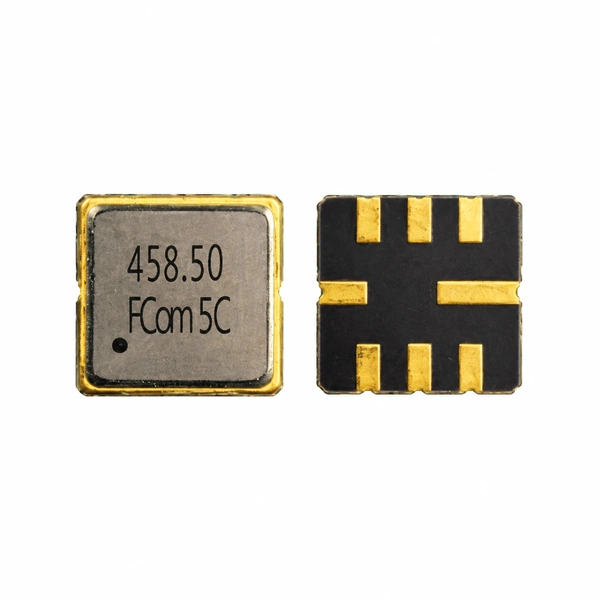
RF signal selection and receiver front-end filtering in a 5.0 × 5.0 mm SMD package.
Key Features
Key Specifications at a Glance
Three characteristics that drive selection for the FSF-5050-458M5: the specified ripple interval, the minimum insertion loss, and the operating temperature range.
Specified ripple interval
448–469 MHz
Amplitude ripple: 0.8 dB typ. / 2.5 dB max. This interval is not a specified 3 dB bandwidth.
Minimum insertion loss
2.0 dB typ.
ILmin: 3.5 dB max. ILmin describes the minimum insertion loss, not the worst-case loss throughout the ripple interval.
Operating temperature
−30 to +60 °C
Storage: −40 to +85 °C. Keep operating and storage limits separate when selecting the part.
The 448–469 MHz interval is the specified ripple interval. Its 21 MHz span must not be relabeled as a 3 dB bandwidth.
Electrical Specifications
Six Key Selection Parameters
“—” means no value is specified for that column; it does not mean zero. Typical values are design guidance. Final production specifications and tolerances are defined by the applicable official test limits and shipment CoC.
Scroll horizontally to view all columns.
| Parameter | Min. | Typ. | Max. | Unit | Definition / condition |
|---|---|---|---|---|---|
| Center frequency | — | 458.5 | — | MHz | Typical |
| Minimum insertion loss, ILmin | — | 2.0 | 3.5 | dB | Minimum insertion loss; not a full-band maximum-loss specification |
| Amplitude ripple | — | 0.8 | 2.5 | dB | 448–469 MHz; specified ripple interval |
| Operating temperature | −30 | — | +60 | °C | Operating limits |
| Storage temperature | −40 | — | +85 | °C | Storage limits; not operating limits |
| Test source / load impedance | — | — | — | Ω | Each 50 Ω; measurement condition, not specified device impedance |
A 3 dB bandwidth value and reference measurement temperature are not provided. The 21 MHz span from 448 to 469 MHz is the specified ripple interval. Device input and output impedances remain unspecified.
Refer to the supplied FCom PDF for the source notes and package drawing. Confirm any additional rejection, return-loss, input-power or DC requirement against the applicable FCom production specification.
Typical Applications
Application Fit
458.5 MHz RF selection
Evaluate the filter for wanted-signal selection around 458.5 MHz, checking the signal band against the ripple and insertion-loss definitions.
Receiver front-end filtering
Use bandpass filtering ahead of later receiver stages. Confirm the required rejection and signal-level limits for the actual receiver.
Custom UHF designs
Consider FSF-5050-458M5 for UHF band selection where its frequency, temperature range and source/load conditions fit the design.
Integration Notes
Confirm the Interface Before PCB Release
Measurement conditions
The supplied measurement configuration uses 50 Ω source and load terminations, with no external matching components shown. These are test conditions; intrinsic device port impedances are not specified.
PCB and signal requirements
Check the actual source/load conditions, ground connections and mounting view against the applicable FCom specification. Include signal level and DC conditions in the design review.
Package & Pin Assignment
Mechanical Interface
The supplied FCom drawing specifies an 8-pad leadless SMD package with a maximum height of 1.5 mm.
Use the datasheet drawing for dimensions and confirm the mounting view before PCB release. The photograph does not define pin orientation.
Pins 2 and 6 retain the FCom Input/Output designation. Confirm signal direction and the complete ordering configuration; contact FCom for other pin-configuration requirements.
| Pin(s) | Function |
|---|---|
| 2 | Input / Output |
| 6 | Input / Output |
| 1, 3 | Ground |
| 5, 7 | Ground |
| 4 | Case ground |
| 8 | Case ground |
Selection and Design-In Support
Discuss Your Signal Path with FCom
Share the required signal band and bandwidth definition, source/load requirements, operating temperature, input signal and DC conditions. Include sample quantity and estimated usage.
Confirm the applicable production test limits, pin configuration and complete ordering code before design release.
Engineering Questions
Frequently Asked Questions
Is the 448–469 MHz interval a 21 MHz 3 dB bandwidth?
No. The interval specifies where the amplitude-ripple limit applies. Although its span is 21 MHz, the supplied FCom document does not provide a 3 dB bandwidth value.
Does the 3.5 dB insertion-loss limit apply across the entire ripple band?
The supplied value is the maximum limit for ILmin, the minimum insertion loss. It is not stated as a worst-case insertion-loss limit at every frequency from 448 to 469 MHz. Evaluate the required signal band against the applicable production specification.
Are the device input and output impedances 50 Ω?
The supplied document specifies a 50 Ω source and load for measurement. Device input and output impedances are not specified. The measurement circuit shows no external matching components; this does not establish a match to every source, load or PCB layout.
What operating and storage temperatures apply?
The operating range is −30 to +60 °C. Storage is specified separately from −40 to +85 °C and must not be used as the operating range. The supplied document does not state a reference measurement temperature.
What are the package and signal pins?
The FCom package is 5.0 × 5.0 mm with eight pads and a maximum height of 1.5 mm. Pins 2 and 6 are labeled Input/Output; pins 1, 3, 5 and 7 are ground, and pins 4 and 8 are case ground. Confirm the mounting view against the applicable drawing before PCB release.
What should I include in a selection inquiry?
Provide the model, required signal band and bandwidth definition, source/load requirements, operating temperature, input signal and DC conditions, sample quantity and estimated usage. Confirm the complete ordering code, production test limits and applicable shipment CoC before design release.