
FCom Fuji Crystal · FSF-5050 Series
390, 391 & 394 MHz SAW Bandpass Filters
FSF-5050-390M · FSF-5050-391M · FSF-5050-394M
Compare three frequency options in a 5.0 × 5.0 mm, 8-pad SMD package for RF signal selection and suitable IF filtering. Select by passband definition, insertion-loss limits and operating temperature; electrical requirements differ by model.
390 MHz data status: draft electrical values pending verification. Confirm the applicable specification before design release.
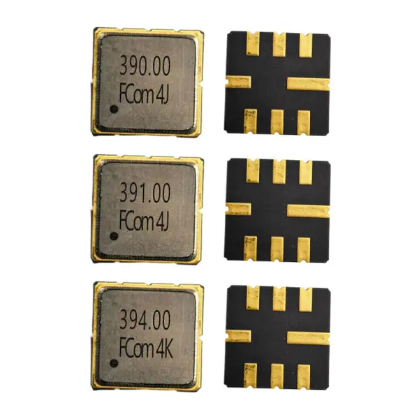
Left: marked cover. Right: pad side. Product photographs are not pad-orientation drawings.
Model Selection
Three models. Distinct requirements.
Passband ranges and 3 dB bandwidth are different specifications. The operating ranges and measurement bands differ; the three models are not established as interchangeable.
Draft data · verification pending
FSF-5050-390M
390 MHz
Typical 3 dB bandwidth 0.5 MHz — passband limits not specified
- Insertion loss
- 1.7 dB typ. / 3.0 dB max.
- Operating range
- −20 to +70 °C
- Amplitude ripple
- Not specified
- Test source / load
- Not specified
Specified passband
FSF-5050-391M
391 MHz
Specified passband 387–395 MHz; 3 dB bandwidth not specified
- Insertion loss
- 2.0 dB typ. / 4.0 dB max.
- Amplitude ripple
- 0.3 dB typ. / 2.0 dB max.
- Operating range
- −30 to +85 °C
- Source / load test
- 50 Ω / 50 Ω
Specified passband
FSF-5050-394M
394 MHz
Specified passband 392–396 MHz; 3 dB bandwidth not specified
- Insertion loss
- 1.7 dB typ. / 3.0 dB max.
- Amplitude ripple
- 0.4 dB typ. / 1.3 dB max.
- Operating range
- −10 to +50 °C
- Source / load test
- 50 Ω / 50 Ω
The 391 MHz and 394 MHz documents specify passband ranges for insertion loss and ripple; they do not specify 3 dB bandwidth. Only the 390 MHz draft lists a typical 3 dB bandwidth of 0.5 MHz, which remains unverified. Source and load conditions for the 390 MHz draft are not specified.
Six key parameters per model
Electrical specifications
“—” means not specified in the supplied data, not zero. Operating temperature limits do not establish the temperature at which every electrical value was measured.
FSF-5050-390M
Scroll horizontally to view all columns.
| Parameter | Min. | Typ. | Max. | Unit | Definition / condition |
|---|---|---|---|---|---|
| Center frequency | — | 390 | — | MHz | FCom draft |
| 3 dB bandwidth | — | 0.5 | — | MHz | FCom draft; passband limits not specified |
| Insertion loss | — | 1.7 | 3.0 | dB | FCom draft; measurement band not specified |
| Amplitude ripple | — | — | — | dB | Not specified |
| Operating temperature | −20 | — | +70 | °C | FCom draft operating limits |
| Test source / load impedance | — | — | — | Ω | Not specified |
All values above are retained from the supplied FCom draft and remain unverified. Passband limits, attenuation, test impedances and matching conditions are not established. Confirm applicable data before design release.
FSF-5050-391M
Scroll horizontally to view all columns.
| Parameter | Min. | Typ. | Max. | Unit | Definition / condition |
|---|---|---|---|---|---|
| Center frequency | — | 391 | — | MHz | Listed under Typ. in the supplied data |
| Specified passband | — | — | — | MHz | 387–395 MHz; not a 3 dB bandwidth |
| Insertion loss | — | 2.0 | 4.0 | dB | Over 387–395 MHz |
| Amplitude ripple | — | 0.3 | 2.0 | dB | Over 387–395 MHz |
| Operating temperature | −30 | — | +85 | °C | Operating range, not a stated measurement temperature |
| Test source / load impedance | — | 50 / 50 | — | Ω | Source / load test terminations |
The supplied FCom document follows reference electrical data. Confirm FCom production limits before design release. A 3 dB bandwidth and a common measurement temperature are not specified.
FSF-5050-394M
Scroll horizontally to view all columns.
| Parameter | Min. | Typ. | Max. | Unit | Definition / condition |
|---|---|---|---|---|---|
| Center frequency | — | 394 | — | MHz | Listed under Typ. in the supplied data |
| Specified passband | — | — | — | MHz | 392–396 MHz; not a 3 dB bandwidth |
| Insertion loss | — | 1.7 | 3.0 | dB | Over 392–396 MHz |
| Amplitude ripple | — | 0.4 | 1.3 | dB | Over 392–396 MHz; unit per supplied FCom data |
| Operating temperature | −10 | — | +50 | °C | Operating range, not a stated measurement temperature |
| Test source / load impedance | — | 50 / 50 | — | Ω | Source / load test terminations |
Ripple is shown in dB as stated in the supplied FCom document; the reference document has a conflicting printed unit. Confirm the applicable FCom production specification. A 3 dB bandwidth and a common measurement temperature are not specified.
Additional attenuation data for 391 MHz and 394 MHz appear in the supplied combined FCom datasheet. Full specifications and release status must be checked against the applicable model document.
Application Fit
Typical applications
RF bandpass filtering
Frequency selection around 390, 391 or 394 MHz when the model’s passband and rejection requirements match the design.
Receiver signal selection
Pass the intended receiver signal band while attenuating signals outside the passband. Evaluate insertion loss within the system gain and noise budget.
Suitable IF stages
Use at an intermediate frequency only when signal bandwidth, operating temperature and source/load conditions are compatible.
Integration Notes
Matching, grounding and PCB evaluation
391 MHz & 394 MHz
The supplied data use 50 Ω source and 50 Ω load test terminations. The referenced measurement circuits show a direct connection without an external matching network; intrinsic device input/output impedances are not specified.
The reference test circuits ground pins 1, 3, 4, 5, 7 and 8. Verify the FCom implementation and grounding against the applicable drawing.
390 MHz
Test source/load impedances and matching conditions are not specified in the supplied draft. Provide the intended interface conditions for confirmation before selecting matching components.
For each model, assess PCB parasitics and signal loading with the actual application circuit. No verified application schematic is supplied here.
Passband ranges in the 391 MHz and 394 MHz data are specified performance intervals for insertion loss and ripple; they are not 3 dB bandwidths. The 390 MHz draft lists a typical 3 dB bandwidth of 0.5 MHz, which remains unverified.
Mechanical Interface
Package & pin assignment
The supplied FCom pages show a 5.0 × 5.0 mm, 8-pad leadless SMD package with a maximum height of 1.5 mm for all three models. Use the applicable FCom mechanical drawing for dimensions and orientation. The photograph does not establish pad numbering or mounting view.
Shared FSF-5050 package
FCom labels pins 2 and 6 Input/Output. Confirm signal direction before PCB release. Contact FCom to discuss other pin-configuration requirements.
The reference measurement circuits ground pins 1, 3, 4, 5, 7 and 8. Verify grounding and pad orientation against the applicable FCom drawing before layout release.
| Pin(s) | FCom function |
|---|---|
| 2 | Input/Output |
| 6 | Input/Output |
| 1, 3, 5, 7 | Ground |
| 4, 8 | Case ground |
Selection and Design-In Support
What to include in your inquiry
Share the required frequency band, bandwidth definition, source/load requirements and temperature range with FCom. Include sample quantity and estimated usage so your inquiry can be evaluated against the appropriate model and specification.
Model names on this page identify the selection options. Confirm the complete ordering code and applicable production limits before ordering. For FSF-5050-390M, request confirmation of electrical limits and matching conditions before design release.
Engineering Questions
Frequently asked questions
How do I choose between the three models?
Choose by center frequency, required passband and operating temperature. FSF-5050-391M specifies a 387–395 MHz passband; FSF-5050-394M specifies 392–396 MHz. The 390 MHz data are draft values pending verification. Similar package dimensions do not establish interchangeability.
Are the specified passbands the same as 3 dB bandwidth?
No. The 391 MHz and 394 MHz documents specify passband ranges for insertion loss and ripple; they do not specify 3 dB bandwidth. Only the 390 MHz draft lists a typical 3 dB bandwidth of 0.5 MHz, which remains unverified.
Do all three models use a 50-ohm test system?
The supplied 391 MHz and 394 MHz data use 50-ohm source and load test conditions. These are test terminations, not a specification of the intrinsic device impedances. Source and load conditions for the 390 MHz draft are not specified.
What should I check before laying out the PCB?
Check the applicable FCom drawing, pad orientation, signal pin assignment, grounding and required matching. The supplied FCom pin table labels pins 2 and 6 Input/Output, pins 1, 3, 5 and 7 ground, and pins 4 and 8 case ground. Confirm direction and footprint before PCB release.
Are all specifications measured at the same temperature?
A common reference measurement temperature is not stated for the three models in the supplied data. The operating ranges are −20 to +70 °C for 390M, −30 to +85 °C for 391M and −10 to +50 °C for 394M. Operating ranges must not be treated as measurement conditions.
What information should I include in an inquiry?
Include the selected model or center frequency, required bandwidth and its definition, source and load requirements, operating temperature, sample quantity and estimated usage. For FSF-5050-390M, request confirmation of electrical limits and matching conditions before design release.