
FCom Fuji Crystal · FSF-5050 Series · SAW Bandpass Filters
387.5, 388 & 388.5 MHz SAW Filters
FSF-5050-387M5 · FSF-5050-388M · FSF-5050-388M5
Three frequency options for RF bandpass filtering, receiver signal selection and suitable IF paths. Select by passband definition, loss budget and operating temperature.
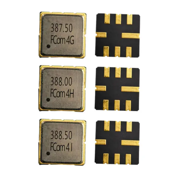
Left: marked top face. Right: underside pads.
Model Selection
Choose the Frequency and Passband Your Design Needs
The bandwidth definitions and loss/ripple intervals differ. A shared package does not establish electrical interchangeability.
2 dB bandwidth
FSF-5050-387M5
387.5 MHz
2 dB bandwidth 7.5 MHz min. / 11.0 MHz typ.
- Insertion loss
- 1.9 dB typ. / 3.0 dB max. over 385–390 MHz
- Amplitude ripple
- 0.5 dB typ. / 2.0 dB max. over 385–390 MHz
- Operating range
- −40 to +85 °C
- Source / load test
- 50 Ω / 50 Ω
For 387.5 MHz paths requiring the listed 2 dB bandwidth and operation down to −40 °C.
Specified passband
FSF-5050-388M
388 MHz
Specified passband 386–390 MHz · no dB bandwidth criterion stated
- Insertion loss
- 1.8 dB typ. / 3.0 dB max. over 386–390 MHz
- Amplitude ripple
- 0.6 dB typ. / 1.3 dB max. over 386–390 MHz
- Operating range
- −10 to +50 °C
- Source / load test
- 50 Ω / 50 Ω
For 388 MHz paths using the 386–390 MHz specified passband within the narrower operating temperature range.
2 dB bandwidth
FSF-5050-388M5
388.5 MHz
2 dB bandwidth 6.5 MHz typ.
- Insertion loss
- 1.4 dB typ. / 3.0 dB max. over 386–389 MHz
- Amplitude ripple
- 0.3 dB typ. / 1.6 dB max. over 386–389 MHz
- Operating range
- −55 to +85 °C
- Source / load test
- 50 Ω / 50 Ω
For 388.5 MHz paths requiring operation down to −55 °C; check the specified 386–389 MHz loss and ripple interval.
Bandwidth definitions and loss/ripple intervals differ across the three models. Model names are identification labels; confirm the complete ordering code with FCom. The supplied 388M and 388M5 pages require FCom production-limit confirmation before design release.
Electrical Specifications
Keep Each Model’s Limits with Its Test Conditions
“—” means no value or condition is stated for that entry. Typical values are not guaranteed limits. The FCom pages do not state a general measurement temperature.
FSF-5050-387M5 · 387.5 MHz
Scroll horizontally to view all columns.
| Parameter | Min. | Typ. | Max. | Unit | Definition / condition |
|---|---|---|---|---|---|
| Center frequency, fc | — | 387.5 | — | MHz | Listed as typical in the supplied FCom table |
| Insertion loss | — | 1.9 | 3.0 | dB | Over 385–390 MHz |
| 2 dB bandwidth | 7.5 | 11.0 | — | MHz | 2 dB criterion; 3 dB bandwidth not specified |
| Amplitude ripple | — | 0.5 | 2.0 | dB | Over 385–390 MHz |
| Operating temperature | −40 | — | +85 | °C | Operating range; not a general measurement temperature |
| Test source / load impedance | — | 50 / 50 | — | Ω | Test terminations; device port impedances not specified |
The 387M5 excludes the TA0964B-only 475–476 MHz rejection requirement. Attenuation in the combined FCom datasheet is referenced to 0 dB, not to minimum insertion loss. Device input and output port impedances are not specified.
FSF-5050-388M · 388 MHz
Scroll horizontally to view all columns.
| Parameter | Min. | Typ. | Max. | Unit | Definition / condition |
|---|---|---|---|---|---|
| Center frequency, fc | — | 388 | — | MHz | Listed as typical in the supplied FCom table |
| Insertion loss | — | 1.8 | 3.0 | dB | Over 386–390 MHz |
| Specified passband | 386 | — | 390 | MHz | Specified interval; not a 3 dB bandwidth |
| Amplitude ripple | — | 0.6 | 1.3 | dB | Over 386–390 MHz |
| Operating temperature | −10 | — | +50 | °C | Operating range; not a general measurement temperature |
| Test source / load impedance | — | 50 / 50 | — | Ω | Test terminations; device port impedances not specified |
The supplied FCom page for 388M requires FCom production-limit confirmation before design release. The reference outline and measurement circuit show inconsistent terminal labeling for this model; confirm the pin mapping against the applicable FCom drawing.
FSF-5050-388M5 · 388.5 MHz
Scroll horizontally to view all columns.
| Parameter | Min. | Typ. | Max. | Unit | Definition / condition |
|---|---|---|---|---|---|
| Center frequency, fc | — | 388.5 | — | MHz | Listed as typical in the supplied FCom table |
| Insertion loss | — | 1.4 | 3.0 | dB | Over 386–389 MHz |
| 2 dB bandwidth | — | 6.5 | — | MHz | 2 dB criterion; 3 dB bandwidth not specified |
| Amplitude ripple | — | 0.3 | 1.6 | dB | Over 386–389 MHz |
| Operating temperature | −55 | — | +85 | °C | Operating range; not a general measurement temperature |
| Test source / load impedance | — | 50 / 50 | — | Ω | Test terminations; device port impedances not specified |
Passband VSWR is 2.0 typical and 2.2 maximum over 386–389 MHz; VSWR is dimensionless. The supplied FCom page for 388M5 requires FCom production-limit confirmation before design release.
The combined FCom datasheet contains the full attenuation tables; attenuation is referenced to 0 dB, not to minimum insertion loss. No approved full ordering code or controlled FCom revision was supplied for these pages.
Typical Applications
RF Selection and Suitable IF Paths
RF Bandpass Filtering
Evaluate the model centered at 387.5, 388 or 388.5 MHz to pass the intended RF signal while reducing signals in the specified attenuation regions.
Receiver Signal Selection
Use the selected filter in a receiver front end after checking passband loss, ripple and rejection against the signal and blocker requirements.
Intermediate-Frequency Filtering
Consider these filters in an IF path only when its center frequency, occupied bandwidth and interface conditions fit the selected model’s specification.
Integration Notes
Confirm the Interface Before PCB Release
50 Ω Test Conditions
All three FCom pages state 50 Ω source and load test terminations. The reference tests show direct connection without external matching components. This does not specify the device port impedances or prove suitability for every 50 Ω circuit.
Grounding and Pin Mapping
Ground pins 1, 3, 4, 5, 7 and 8 for testing, including both case grounds. Confirm orientation and signal-pin mapping for the intended FCom device. The 388M reference shows inconsistent terminal labeling between its measurement circuit and outline.
Board Evaluation
Evaluate insertion loss, ripple, rejection and impedance behavior on the intended PCB with the agreed test conditions. Confirm the required single-ended or differential interface and any application-specific matching before release.
Shared FCom Package
Package & Pin Assignment
These dimensions and pin functions apply to all three models in the supplied FCom datasheet, pages 1–3.
5.0 × 5.0 mm · Eight-Pad SMD
Maximum height: 1.5 mm. No-lead package.
Use the applicable FCom dimensional drawing to confirm pad numbering and viewing direction. The supplied package drawing is not a separately approved PCB land pattern; obtain the applicable layout requirements before PCB release.
For alternative pin configurations, contact FCom.
| Pin(s) | Function |
|---|---|
| 2 | Input/Output |
| 6 | Input/Output |
| 1, 3, 5, 7 | Ground |
| 4, 8 | Case Ground |
Selection and Design-In Support
Bring the Signal and Interface Requirements Together
Contact FCom to discuss the selected model, required bandwidth and criterion, source/load requirements, temperature and application. Include sample quantity and estimated annual volume. Confirm the production specification, package information and full ordering code as part of the review.
Engineering Questions
Frequently Asked Questions
How do I choose among the three models?
Start with the required center frequency, then compare the specified loss and ripple interval, bandwidth definition and operating temperature. The 388M is limited to −10 to +50 °C; the 387M5 covers −40 to +85 °C and the 388M5 covers −55 to +85 °C. Similar frequencies and a shared package do not establish interchangeability.
Are the bandwidth values directly comparable?
No. The 387M5 specifies 2 dB bandwidth of 7.5 MHz minimum and 11.0 MHz typical; the 388M5 specifies 6.5 MHz typical at 2 dB. The 388M specifies a 386–390 MHz passband without a dB bandwidth criterion. None of the three FCom datasheet pages specifies 3 dB bandwidth.
Does a 50 Ω test termination mean the device ports are 50 Ω?
No. All three models list 50 Ω source and load test terminations, and the referenced test circuits show no external matching components. Device input and output impedances are not specified. Confirm the interface, pin mapping and response on the intended PCB before design release.
Does the 387M5 include the additional 475–476 MHz rejection limit?
No. The FCom datasheet uses the shared TA0964A/B limits and explicitly excludes the TA0964B-only rejection requirement at 475–476 MHz. Use the attenuation limits stated in the FCom datasheet for this model.
What package and pin assignment apply?
The supplied FCom information lists a 5.0 × 5.0 mm, eight-pad, no-lead SMD package with 1.5 mm maximum height for all three models. Pins 2 and 6 are Input/Output; pins 1, 3, 5 and 7 are Ground; pins 4 and 8 are Case Ground. Confirm viewing direction and pad orientation against the applicable FCom drawing before layout.
What should I confirm before ordering?
Confirm the applicable FCom production specification, test conditions and complete ordering code. The supplied 388M and 388M5 pages specifically require production-limit confirmation before design release. Include the selected model, required bandwidth, source/load requirements, operating temperature, application, sample quantity and expected volume in your inquiry.