
FCom Fuji Crystal · FSF-5050 Series
372.5 MHz SAW Bandpass Filter
FSF-5050-372M5
RF and IF receiver filtering at 372.5 MHz, with a specified 3 dB bandwidth and external matching in the reference test.
Review the ILmin-based response limits and −45 to +120 °C operating range, then confirm the matching and FCom pin connections for your design.
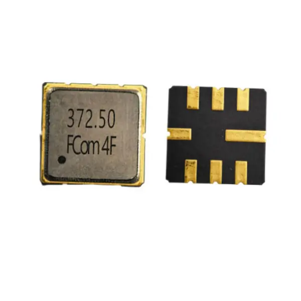
Key Features
Check the response and temperature requirements
3 dB bandwidth
670 kHz min.
1050 kHz typical, measured relative to ILmin. No maximum bandwidth is specified.
Minimum insertion loss
2.5 dB typ.
4.0 dB maximum for ILmin, measured over 372.35–372.65 MHz.
Operating temperature
−45 to +120 °C
Evaluate the documented operating range together with the required interface and production limits.
Electrical Specifications
Keep ILmin and relative loss distinct
Six key specifications from the supplied FCom datasheet. “—” means a value is not specified; it does not mean zero. Typical values are for design guidance.
Scroll horizontally to view all columns.
| Parameter | Min. | Typ. | Max. | Unit | Definition / condition |
|---|---|---|---|---|---|
| Center frequency | — | 372.5 | — | MHz | fC |
| Minimum insertion loss | — | 2.5 | 4.0 | dB | ILmin; measured over 372.35–372.65 MHz |
| 3 dB bandwidth | 670 | 1050 | — | kHz | BW3; relative to ILmin |
| Passband loss | — | 1.0 | 2.0 | dB | 372.34–372.66 MHz; relative to ILmin |
| Passband loss | — | — | 3.0 | dB | 372.32–372.68 MHz; relative to ILmin |
| Operating temperature | −45 | — | +120 | °C | Operating limits |
Amplitude ripple is not specified. The two passband-loss rows are relative to ILmin and must not be treated as ripple specifications or absolute insertion-loss limits. A general measurement temperature is not stated.
The documented reference uses 50 Ω source and load with external matching. Confirm the network and its mapping to FCom signal pins before implementing the test circuit.
Typical Applications
Filtering in a 372.5 MHz receiver path
RF receiver front-end selection
Evaluate FSF-5050-372M5 for bandpass filtering at 372.5 MHz. Review the signal bandwidth, relative passband-loss limits and attenuation intervals against the receiver requirements.
IF filtering with external matching
Use the documented response as a starting point for an IF stage at 372.5 MHz. Include the external matching in the interface review and confirm the applicable FCom pin connections before board evaluation.
Integration Notes
Confirm the matched interface before layout
Reference matching network
The reference test uses a 50 Ω source and load. Each port has a series 47 nH inductor and a shunt 7 pF capacitor on the analyzer side of that inductor.
Device input and output impedances are unspecified. The test terminations do not establish direct 50 Ω device compatibility.
The reference measurement circuit uses pins 2 and 5; its outline page and the supplied FCom pin table identify signal pins 2 and 6. Confirm the applicable mapping before transferring the network or ground connections.
Ratings and response references
The supplied FCom document lists maximum input power of 10 dBm, a DC voltage rating of 0 V, and storage temperature from −45 to +120 °C. Respect the 0 V DC condition when reviewing the interface.
Stopband attenuation is relative to ILmin, not to an absolute 0 dB reference. See the FCom datasheet for all six frequency ranges and limits.
The turnover temperature is 25 °C typical. This is not a general measurement-temperature statement and must not be applied as a test condition for the entire table.
FCom Package and Connections
Package & Pin Assignment
5.0 × 5.0 mm · 1.5 mm max. height
The supplied FCom drawing specifies an eight-pad, no-lead SMD package for FSF-5050-372M5.
Use the FCom pin functions shown opposite. Confirm the viewing direction, pad numbering and PCB land pattern before layout release. The product photograph is not a placement drawing.
A matching reference or third-party outline does not establish pin-for-pin interchangeability. Contact FCom for the applicable configuration and alternative pin requirements.
| Pin(s) | Function |
|---|---|
| 2 | Input / Output |
| 6 | Input / Output |
| 1, 3, 5, 7 | Ground |
| 4, 8 | Case ground |
Selection and Design-In Support
What to include in your inquiry
Share your bandwidth and loss criteria, source and load, operating temperature and application with FCom. Include sample quantity and estimated usage, and confirm the matching, pin mapping, production limits and complete ordering code.
Engineering Questions
Frequently Asked Questions
What does the specified 3 dB bandwidth mean?
The 3 dB bandwidth is measured relative to minimum insertion loss, ILmin. The FCom datasheet lists 670 kHz minimum and 1050 kHz typical, with no maximum specified. These bandwidth values are separate from the narrower frequency intervals used for passband-loss limits.
Are the passband-loss values amplitude ripple?
No. Over 372.34–372.66 MHz, passband loss relative to ILmin is 1.0 dB typical and 2.0 dB maximum. Over 372.32–372.68 MHz, it is 3.0 dB maximum, with no typical value stated. Amplitude ripple is not specified in the supplied FCom datasheet.
What does minimum insertion loss describe?
ILmin is the minimum insertion loss measured over 372.35–372.65 MHz. Its specified values are 2.5 dB typical and 4.0 dB maximum. The word “minimum” is part of the measurement definition; it does not make 2.5 dB a minimum acceptance limit or establish loss across the entire passband.
Can I connect the filter directly to a 50 Ω circuit?
The documented 50 Ω test uses external matching at both ports: a series 47 nH inductor and a shunt 7 pF capacitor on the analyzer side of each inductor. Device input and output impedances are not specified. Confirm the matching and its mapping to the supplied FCom pins before PCB evaluation; direct connection is not the documented test condition.
Why must the reference pin mapping be confirmed?
The FCom pin table lists pins 2 and 6 as Input/Output. The referenced measurement circuit uses signal pins 2 and 5, while its outline page identifies pins 2 and 6. Confirm the applicable FCom connections and matching before using the reference circuit. Do not transfer the reference ground connections without resolving the signal-pin mapping.
What should I include in an inquiry?
Include FSF-5050-372M5 or the required frequency, bandwidth and loss criteria, source and load requirements, operating temperature, application, sample quantity and estimated usage. Ask to confirm the applicable pin mapping, matching network, production limits and complete ordering code.