
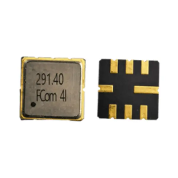
FCom Fuji Crystal · FSF-5050-291M4
291.4 MHz IF SAW Bandpass Filter
FSF-5050-291M4
Select the wanted IF band before downstream amplification or conversion. FSF-5050-291M4 specifies insertion loss and ripple over 287.9–294.9 MHz in a 5.0 × 5.0 mm SMD package.
Selection Essentials
Defined signal band and matching conditions
Specified passband
287.9–294.9 MHz
A 7 MHz interval over which insertion loss and amplitude ripple are specified. Check that the required signal band fits these endpoints.
Matched test interface
50 Ω source / load
The test setup includes a series 8 pF capacitor and a shunt 47 nH inductor at each signal port. Keep these conditions with the electrical data.
3 dB bandwidth: — (not specified). The 7 MHz specified interval is not a measured 3 dB bandwidth. Confirm the bandwidth definition needed by the receiver before selecting a filter.
Six Key Parameters
Electrical specifications
FCom FSF-5050-291M4. Retain the stated source/load and matching conditions when evaluating insertion loss, ripple and rejection.
Scroll horizontally to view all columns.
| Parameter | Min. | Typ. | Max. | Unit | Definition / condition |
|---|---|---|---|---|---|
| Center frequency | — | 291.4 | — | MHz | Fc; no frequency-tolerance limits are specified |
| Specified passband | 287.9 | — | 294.9 | MHz | Fc ±3.5 MHz; interval for insertion loss and ripple; not a 3 dB bandwidth |
| Insertion loss | — | 3.0 | 4.5 | dB | Over 287.9–294.9 MHz |
| Amplitude ripple | — | 0.85 | 2.0 | dB | Over 287.9–294.9 MHz |
| Operating temperature | −10 | — | +50 | °C | Operating limits; storage limits are separate |
| Source / load test termination | — | 50 / 50 | — | Ω | With series 8 pF C and shunt 47 nH L at each signal port |
The electrical-characteristic test temperature is not stated. Typical values are for design guidance and do not become guaranteed limits across the operating range. “—” means not specified. Complete stopband limits, package details and pin functions are in the one-page FCom product document.
Stopband attenuation is absolute. The minimum is 40 dB over 191.4–253.9 MHz and 328.9–391.4 MHz; typical values are 55 dB and 65 dB, respectively. The 0 dB reference differs from a passband-relative rejection value. These values are not additional rejection relative to the passband loss and do not describe every frequency outside the specified passband. Evaluate the stated frequency intervals against the receiver’s blocker frequencies.
Typical Applications
Band selection in a 291.4 MHz IF path
Receiver IF filtering
Use the 291.4 MHz center frequency to align the filter with the receiver’s intermediate-frequency plan.
Channel-band selection
Assess wanted-signal loss and ripple within 287.9–294.9 MHz, keeping the required bandwidth definition explicit.
Out-of-band rejection
Evaluate the specified stopband attenuation before downstream IF amplification or conversion.
- IF source stage
Actual source impedance - FSF-5050-291M4
Input matching · SAW filter · output matching - IF amplifier / converter
Actual load impedance
Functional application example. Matching is included at both ports; this diagram does not specify component placement or a validated PCB circuit.
Design-In Essentials
Check matching, ratings and handling
Interface and PCB evaluation
- Reference test conditions: 50 Ω source and load, with a series 8 pF capacitor and a shunt 47 nH inductor at each signal port.
- Device input/output impedances: — (not specified). The 50 Ω test terminations do not establish native 50 Ω device ports.
- Check the actual source/load impedances, component tolerances, grounding and PCB layout before finalizing the interface.
Limits and handling
- Maximum RF input power: 5 dBm. Maximum DC voltage: 3 V.
- Operating temperature: −10 to +50 °C. Storage temperature: −40 to +85 °C.
- Maximum ratings are limits, not recommended operating targets.
- ESD-sensitive device: use appropriate ESD-controlled handling and assembly practices.
Package and Connections
Package & pin assignment
5.0 × 5.0 mm
1.5 mm maximum height · 8-pad SMD, no lead
Dimensions and pin functions follow the FSF-5050-291M4 FCom document. Confirm the drawing orientation and applicable footprint before PCB release; the function table does not assign an unverified top or bottom view. For other pin configurations, contact FCom to discuss the requirement.
| Pin(s) | Function |
|---|---|
| 2 | Input/Output |
| 6 | Input/Output |
| 1, 3, 5, 7 | Ground |
| 4, 8 | Case Ground |
Selection and Design-In Support
Share the signal band and interface requirements
Include the required passband, bandwidth definition, source/load conditions and operating temperature. Add sample quantity, estimated usage and blocker-frequency targets for a focused selection discussion.
Confirm the complete ordering code and applicable specification with FCom before ordering.
Selection Questions
Frequently Asked Questions
Is the 7 MHz specified passband a 3 dB bandwidth?
No. The 287.9–294.9 MHz interval, or Fc ±3.5 MHz, specifies where insertion loss and amplitude ripple apply. Its span is 7 MHz. A 3 dB bandwidth and measured 3 dB cutoff frequencies are not specified in the supplied document.
Does a 50 Ω test system mean the filter needs no matching?
No. The specified measurement setup uses 50 Ω source and load, with a series 8 pF capacitor and a shunt 47 nH inductor at each signal port. Device input and output impedances are not specified. Evaluate the stated network with the actual circuit source, load, components and PCB layout.
What input-power, voltage and temperature limits apply?
Maximum RF input power is 5 dBm and maximum DC voltage is 3 V. The operating temperature range is −10 to +50 °C; storage is −40 to +85 °C. Maximum ratings are limits, not recommended operating targets. The storage range does not extend the operating range.
How should the stopband attenuation be interpreted?
The stopband attenuation is absolute, referenced to 0 dB. The minimum is 40 dB over 191.4–253.9 MHz and 328.9–391.4 MHz; typical values are 55 dB and 65 dB, respectively. These values are not additional rejection relative to the passband loss and do not describe every frequency outside the specified passband.
Which pads carry the signal and ground connections?
The FCom document identifies pins 2 and 6 as Input/Output, pins 1, 3, 5 and 7 as Ground, and pins 4 and 8 as Case Ground. Confirm the applicable drawing orientation, routing and footprint before PCB release. The shared FSF-5050 package format alone does not establish interchangeability with another frequency model.
What should I include in a technical inquiry?
Specify FSF-5050-291M4 or a 291.4 MHz center frequency, the required passband and bandwidth definition, source/load requirements, operating temperature, sample quantity and estimated usage. Add blocker frequencies and rejection targets when relevant. Confirm the complete ordering code and applicable specification with FCom before ordering.