
FSF-5050 series · 8-pad SMD
200 MHz Narrowband SAW Bandpass Filter
FSF-5050-200M
Narrowband filtering for 200 MHz receiver and RF / IF measurement stages, with a 150 kHz minimum 1 dB bandwidth in a compact 5.0 × 5.0 mm package.
Key Features
Narrowband performance in a compact SMD package
Bandwidth, passband level and attenuation use different definitions. The passband and all six attenuation intervals are referenced to ILmin.
1 dB bandwidth
150 kHz min.
390 kHz typical
3 dB bandwidth
469 kHz typ.
Minimum value not specified
Minimum insertion loss
2.0 dB typ.
ILmin: 3.5 dB maximum; includes matching-component loss
Operating temperature
−20 to +70 °C
Specified operating range
Electrical Specifications
Electrical specifications
Bandwidth, passband level and attenuation use different definitions. The passband and all six attenuation intervals are referenced to ILmin.
Scroll horizontally to view all columns.
| Parameter | Min. | Typ. | Max. | Unit | Condition / frequency interval |
|---|---|---|---|---|---|
| Center frequency | — | 200.00 | — | MHz | Value in the Typ. column of the FCom datasheet |
| Minimum insertion loss (ILmin) | — | 2.0 | 3.5 | dB | Includes matching-component loss |
| 1 dB bandwidth | 150 | 390 | — | kHz | 1 dB bandwidth definition |
| 3 dB bandwidth | — | 469 | — | kHz | Typical value only; minimum not stated |
| Passband level relative to ILmin | — | 0.5 | 1.5 | dB | 199.925–200.075 MHz |
| Relative attenuation | 50 | 60 | — | dB | 10–165 MHz; relative to ILmin |
| Relative attenuation | 33 | 40 | — | dB | 165–195 MHz; relative to ILmin |
| Relative attenuation | 15 | 22 | — | dB | 195–199 MHz; relative to ILmin |
| Relative attenuation | 10 | 25 | — | dB | 201–215.5 MHz; relative to ILmin |
| Relative attenuation | 39 | 46 | — | dB | 215.5–325.5 MHz; relative to ILmin |
| Relative attenuation | 50 | 55 | — | dB | 325.5–1000 MHz; relative to ILmin |
| Operating temperature | −20 | — | +70 | °C | Operating range |
| Storage temperature | −40 | — | +85 | °C | Storage range; not the operating range |
| Maximum input power | — | — | 10 | dBm | Maximum input rating |
| DC voltage | 0 | V | Specified DC voltage rating | ||
| Source / load terminations | 50 / 50 | Ω | Test terminations; external matching required | ||
“—” means no value is stated. The FCom datasheet does not state a separate measurement temperature. Operating and storage temperature ranges are listed separately.
Passband definition: 0.5 dB typical / 1.5 dB maximum over 199.925–200.075 MHz describes the level relative to ILmin. It is not specified as peak-to-peak ripple or as a 3 dB bandwidth.
Typical Applications
Typical applications
01 / NARROWBAND RECEIVERS
200 MHz receive filtering
Select signals around 200 MHz and assess out-of-band suppression against the listed attenuation intervals. Check occupied-band loss against the actual signal requirements.
02 / INTERMEDIATE FREQUENCY
IF channel selection
Provide narrowband filtering in a superheterodyne receiver using a 200 MHz IF. Evaluate the required signal bandwidth against both the bandwidth limits and the fixed passband interval.
03 / MEASUREMENT SYSTEMS
RF / IF signal conditioning
Apply frequency selection in a 200 MHz measurement signal path. Include the matching network and its loss when evaluating the complete chain.
Integration Notes
Matching & integration
Each port uses a 220 nH series inductor and a 0.2 pF shunt capacitor at the filter-side node. The 50 Ω labels describe the external source and load terminations.
Reference matching components
The FCom datasheet lists Coilcraft 0805 CS series inductors and Murata 0402 GRM series capacitors as the reference components.
Evaluate alternative components and PCB placement with the complete filter network. The specified insertion loss already includes matching-component loss.
Board-level checks
- Keep RF interconnects short and provide appropriate ground paths at the matching capacitors and ground pads.
- Check the actual RF input level and ensure the specified 0 V DC condition at the filter.
- Verify the response over the required signal band and operating conditions.
- Confirm pin orientation and the complete ordering code before releasing the design.
Electrical connection illustration from the specified matching arrangement. This is not a PCB footprint or a pin-orientation drawing; confirm physical connections using the FCom package drawing.
Package & Pin Assignment
Package & pin assignment
5.0 × 5.0 mm
8-pad SMD · 1.5 mm max height
Use the dimensioned FCom drawing to review mechanical fit. Confirm the drawing orientation before assigning PCB pads.
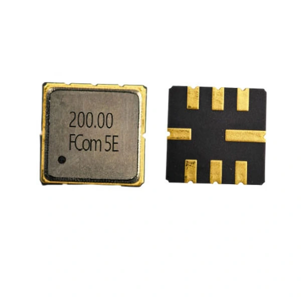
Pins 2 and 6 retain the Input/Output designation shown in the FCom pin table. The product photograph is for identification, not pad-location definition.
Please contact FCom if a different pin configuration is required.
| Pin number | Function |
|---|---|
| 2 | Input / Output |
| 6 | Input / Output |
| 1, 3, 5, 7 | Ground |
| 4, 8 | Case Ground |
Selection and Design-In Support
Selection and design-in support
Share the receiver or measurement requirements with FCom to review FSF-5050-200M for the intended signal path.
Signal requirements
Center frequency, occupied bandwidth, passband limits and attenuation targets.
Interface and environment
Source / load conditions, matching components, input level and temperature range.
Evaluation and ordering
Sample quantity, estimated annual usage and confirmation of the complete ordering code.
Engineering Questions
Frequently asked questions
Is 150 kHz the 3 dB bandwidth?
No. The minimum 1 dB bandwidth is 150 kHz, with a typical value of 390 kHz. The 3 dB bandwidth is specified separately as 469 kHz typical; no minimum 3 dB bandwidth is stated.
What does the 199.925–200.075 MHz passband specification mean?
Within that fixed frequency interval, the passband level is specified relative to ILmin: 0.5 dB typical and 1.5 dB maximum. This is not labeled as peak-to-peak ripple, and it must not be substituted for the 1 dB or 3 dB bandwidth definitions.
Does the insertion loss include the matching components?
Yes. The minimum insertion loss, ILmin, includes the loss of the matching components. It is specified as 2.0 dB typical and 3.5 dB maximum. This ILmin limit is not a maximum-loss guarantee at every frequency across the passband.
Can I omit the matching network in a 50 Ω system?
External matching is required. The 50 Ω values describe the source and load terminations. Each filter port uses a 220 nH series inductor and a 0.2 pF shunt capacitor at the filter-side node, as specified in the FCom datasheet.
What input power and DC limits apply?
The maximum input power is 10 dBm and the specified DC voltage is 0 V. Review both RF level and DC conditions at the filter connections when integrating it into the receiver or measurement circuit.
What should I include in a design-in inquiry?
Include FSF-5050-200M, the required signal bandwidth around 200 MHz, passband and attenuation targets, source and load requirements, RF input level, operating temperature, sample quantity and estimated annual usage. Confirm the complete ordering code with FCom before placing an order.