
FCom Fuji Crystal · FSF-5050 Series · SAW Filter
180.175 / 184 / 188.175 MHz SAW Bandpass Filters
FSF-5050-180M175 · FSF-5050-184M · FSF-5050-188M175
Three models for receiver RF and IF stages. Select the frequency your receiver requires, then compare bandwidth, insertion loss, attenuation intervals and operating temperature.
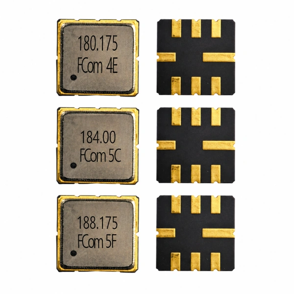
Choose the required frequency
Three models, separate specifications
All three use the same package size. Frequency, temperature coverage and attenuation intervals remain model-specific.
SAW Filter · 180.175 MHz
FSF-5050-180M175
180.175 MHz
3 dB bandwidth: 6.0 MHz min. / 8.9 MHz typ.
- Insertion loss (ILmin)
- 1.55 dB typ. / 2.8 dB max.
- Operating temperature
- −40 to +85 °C
- Upper attenuation interval
- fC +30 to +100 MHz
SAW Filter · 184 MHz
FSF-5050-184M
184 MHz
3 dB bandwidth: 6.0 MHz min. / 9.0 MHz typ.
- Insertion loss (ILmin)
- 1.6 dB typ. / 2.8 dB max.
- Operating temperature
- −40 to +85 °C
- Upper attenuation interval
- fC +30 to +50 MHz
SAW Filter · 188.175 MHz
FSF-5050-188M175
188.175 MHz
3 dB bandwidth: 6.0 MHz min. / 8.9 MHz typ.
- Insertion loss (ILmin)
- 1.62 dB typ. / 2.8 dB max.
- Operating temperature
- −25 to +85 °C
- Upper attenuation interval
- fC +30 to +100 MHz
Read the limits in context. ILmin is the minimum insertion loss of the response. A 2.8 dB maximum ILmin does not specify the maximum loss at every frequency in the 3 dB band. Passband ripple is not specified.
Electrical Specifications
Electrical specifications
All values are from the applicable FCom datasheet page. Electrical specifications apply with 50 Ω source and load terminations; all attenuation figures below are relative to ILmin.
Scroll horizontally to view all columns.
FSF-5050-180M175
180.175 MHz · FCom datasheet, page 1 · 50 Ω source / 50 Ω load
| Parameter | Min. | Typ. | Max. | Unit | Condition / frequency interval |
|---|---|---|---|---|---|
| Center frequency | — | 180.175 | — | MHz | Value in the Typ. column of the FCom datasheet |
| Insertion loss (ILmin) | — | 1.55 | 2.8 | dB | Minimum loss of the response; not a full-band loss limit |
| 3 dB bandwidth | 6.0 | 8.9 | — | MHz | Minimum and typical bandwidth values |
| Relative attenuation · lower interval 1 | 42 | 55 | — | dB | fC −50 to −30 MHz (130.175–150.175 MHz); relative to ILmin |
| Relative attenuation · lower interval 2 | 36 | 52 | — | dB | fC −30 to −15 MHz (150.175–165.175 MHz); relative to ILmin |
| Relative attenuation · upper interval | 42 | 46 | — | dB | fC +30 to +100 MHz (210.175–280.175 MHz); relative to ILmin |
| Operating temperature | −40 | — | +85 | °C | Specified operating range |
FSF-5050-184M
184 MHz · FCom datasheet, page 2 · 50 Ω source / 50 Ω load
| Parameter | Min. | Typ. | Max. | Unit | Condition / frequency interval |
|---|---|---|---|---|---|
| Center frequency | — | 184.0 | — | MHz | Value in the Typ. column of the FCom datasheet |
| Insertion loss (ILmin) | — | 1.6 | 2.8 | dB | Minimum loss of the response; not a full-band loss limit |
| 3 dB bandwidth | 6.0 | 9.0 | — | MHz | Minimum and typical bandwidth values |
| Relative attenuation · lower interval 1 | 42 | 54 | — | dB | fC −50 to −30 MHz (134–154 MHz); relative to ILmin |
| Relative attenuation · lower interval 2 | 36 | 52 | — | dB | fC −30 to −15 MHz (154–169 MHz); relative to ILmin |
| Relative attenuation · upper interval | 42 | 51 | — | dB | fC +30 to +50 MHz (214–234 MHz); relative to ILmin |
| Operating temperature | −40 | — | +85 | °C | Specified operating range |
The 184M upper attenuation interval ends at fC +50 MHz, whereas the other two models extend to fC +100 MHz. Do not apply one model’s attenuation interval to another.
FSF-5050-188M175
188.175 MHz · FCom datasheet, page 3 · 50 Ω source / 50 Ω load
| Parameter | Min. | Typ. | Max. | Unit | Condition / frequency interval |
|---|---|---|---|---|---|
| Center frequency | — | 188.175 | — | MHz | Value in the Typ. column of the FCom datasheet |
| Insertion loss (ILmin) | — | 1.62 | 2.8 | dB | Minimum loss of the response; not a full-band loss limit |
| 3 dB bandwidth | 6.0 | 8.9 | — | MHz | Minimum and typical bandwidth values |
| Relative attenuation · lower interval 1 | 42 | 55 | — | dB | fC −50 to −30 MHz (138.175–158.175 MHz); relative to ILmin |
| Relative attenuation · lower interval 2 | 36 | 52 | — | dB | fC −30 to −15 MHz (158.175–173.175 MHz); relative to ILmin |
| Relative attenuation · upper interval | 42 | 46 | — | dB | fC +30 to +100 MHz (218.175–288.175 MHz); relative to ILmin |
| Operating temperature | −25 | — | +85 | °C | Specified operating range. Lower limit is −25 °C, not −40 °C. |
“—” means no value is stated. Frequency offsets are relative to each model’s center frequency; the absolute intervals are calculated from those offsets. Typical 3 dB bandwidth does not define guaranteed passband edges. The datasheets do not state a separate measurement temperature.
Typical Applications
Typical applications
01 / RECEIVER RF STAGES
VHF preselection
Provide bandpass filtering around the selected center frequency in a receiver front end or monitoring module. Check rejection only within the attenuation intervals specified for that model.
02 / INTERMEDIATE FREQUENCY
RF / IF signal conditioning
Use the model that matches the planned RF or IF filtering stage. Assess the occupied signal bandwidth and loss requirements; the typical 3 dB bandwidth alone does not establish passband flatness.
03 / TELEMETRY RECEIVERS
Remote-monitoring modules
Support frequency selection in telemetry receiver signal chains. Confirm the required environmental range, particularly when the design must operate below −25 °C.
Integration Notes
Integration notes
Review the 50 Ω interface
The stated performance uses 50 Ω source and load terminations. The FCom datasheets do not provide device impedance models or matching component values for these three models.
Confirm the interface and any matching requirements with FCom using your actual receiver circuit and PCB conditions.
- Source termination
- 50 Ω
- Load termination
- 50 Ω
- Passband ripple
- Not specified
- Attenuation reference
- Relative to ILmin
Check the complete receiver path
- Select the correct center frequency before comparing bandwidth or typical loss.
- Keep RF traces short and provide suitable ground connections for all ground and case-ground pads.
- Confirm pin orientation and signal direction before routing the PCB.
- Evaluate occupied-band loss and rejection on the assembled board under the required conditions.
- Confirm the complete ordering code before releasing the bill of materials.
Package & Pin Assignment
Package & pin assignment
The dimensions and pin table below apply to FSF-5050-180M175, FSF-5050-184M and FSF-5050-188M175.
5.0 × 5.0 mm
8-pad SMD · 1.5 mm max height
Review the dimensioned drawing on the applicable FCom datasheet page for mechanical fit. Confirm drawing orientation before assigning PCB pads.
The photographs show product views for identification. A shared outline and pin table do not establish electrical interchangeability.
Please contact FCom if a different pin configuration is required.
| Pin number | Function |
|---|---|
| 2 | Input / Output |
| 6 | Input / Output |
| 1, 3, 5, 7 | Ground |
| 4, 8 | Case Ground |
Selection and Design-In Support
Selection and design-in support
Share the receiver requirements with FCom to review the selected model and its application conditions.
Signal requirements
Center frequency, occupied bandwidth, loss budget and attenuation targets.
Interface and environment
Source / load requirements, board constraints and operating temperature.
Evaluation and ordering
Sample quantity, estimated annual usage and the required ordering-code confirmation.
Engineering Questions
Frequently asked questions
How should I choose between the three models?
Start with the frequency required by your receiver: 180.175, 184 or 188.175 MHz. Then check the 3 dB bandwidth, attenuation ranges and temperature rating. FSF-5050-180M175 and FSF-5050-184M are specified from −40 to +85 °C; FSF-5050-188M175 is specified from −25 to +85 °C. A shared package does not make the models interchangeable.
Does the typical 3 dB bandwidth define a guaranteed flat passband?
No. The 3 dB bandwidth is specified as 6.0 MHz minimum for all three models, with typical values of 8.9 or 9.0 MHz. Passband ripple is not specified. Do not use the typical bandwidth to create guaranteed passband edges or a flatness limit.
Does 2.8 dB maximum insertion loss apply at every frequency in the 3 dB band?
No. The datasheets define insertion loss as ILmin, the minimum insertion loss of the response. The 2.8 dB maximum limit applies to ILmin, not to every frequency across the 3 dB bandwidth.
What is the reference for the attenuation figures?
All attenuation values on this page are relative to ILmin. Each limit applies only to its listed frequency-offset interval. In particular, the upper interval for FSF-5050-184M ends at fC +50 MHz, while the other two models are specified to fC +100 MHz.
Do the 50 Ω source and load specifications eliminate the need to check matching?
No. The FCom datasheets specify performance with 50 Ω source and load terminations, but do not provide device port impedance models or matching component values. Confirm the interface and any matching requirements for the actual PCB with FCom.
What information is needed for a design-in inquiry?
Include the selected model, required frequency and signal bandwidth, attenuation targets, source and load requirements, operating temperature, application, sample quantity and estimated annual usage. Confirm the complete ordering code with FCom before placing an order.