RF Design · Practical Guide
A SAW filter’s response depends on the surrounding RF circuit as well as the component. PCB coupling can reduce rejection, ground inductance can change matching, and an ESD protection device can add unwanted loading. Treat the filter, matching network, protection circuit and board as one design.
FCom Fuji Crystal · Technical Guide
1. Start with the filter and interface requirements
Confirm center frequency, usable bandwidth, insertion loss, rejection bands, port impedances, power limits, temperature range and pin functions. Check whether ports are single-ended or balanced. Do not assume that every SAW filter has two 50 Ω ports or that every unused-looking pad should be grounded.
Obtain the package land pattern, recommended matching circuit and available S-parameters. Record the reference impedance, test fixture and matching conditions associated with the specified response. A matching network is meaningful only with its stated source and load.
SAW devices contain fine electrode structures on a piezoelectric substrate. An electrostatic discharge arriving through an antenna or exposed connection can damage those structures. Out-of-band RF rejection does not establish ESD immunity. [1]
2. Route the RF path and matching network
Choose the board stackup before fixing RF trace dimensions. Characteristic impedance depends on dielectric height and permittivity, copper thickness, trace width and surrounding ground geometry. Use the actual fabrication stackup; a trace width copied from another board may produce a different impedance. [2]
- Keep the filter and its matching components close, with compact connections and minimal unnecessary layer changes.
- Maintain the intended reference plane beneath RF transmission lines; avoid crossing plane gaps.
- Include pads, transitions, protection devices and electrically significant traces in the matching model.
- Avoid long branches for test points or optional components. Unpopulated footprints still introduce parasitics.
- Keep clock lines and switching nodes away from the filter input, output and matching components.
For balanced ports, preserve the manufacturer’s required differential geometry and symmetry. Do not apply a single-ended 50 Ω layout rule to each conductor without checking the intended differential impedance.
3. Control grounding and input-to-output coupling
Give each designated filter ground pad a short connection to the RF reference plane, using nearby vias as the package layout permits. Avoid joining all ground pads through a narrow top-layer connection and one distant via. Shared return impedance can couple the input signal into the output and reduce stopband rejection. [3]
Separate input and output traces instead of routing them alongside one another. Consider coupling between matching inductors as well; spacing and orientation can matter. Follow the device-specific ground pattern, including any local copper clearances. A blanket top-layer ground pour is not a substitute for correct return-current paths.
Ground stitching can improve local connections and isolation, but there is no universal via spacing or count for every filter. Package geometry, stackup and the highest frequency requiring rejection determine what must be modeled and measured. [3]
4. Place protection at the ESD entry point
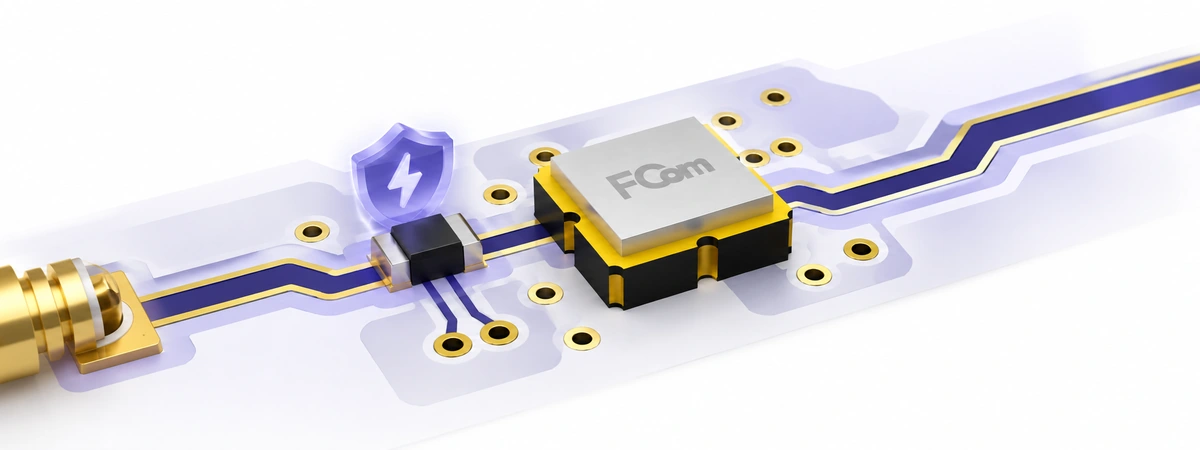
Identify where a discharge can enter: an antenna connector, exposed contact or cable interface. Place the shunt protection device near that entry point, before the transient travels across sensitive circuitry. Route the signal through the protection pad location rather than connecting the suppressor by a long branch. [4] [5]
The discharge-current return must also be short and low in inductance. Use a compact ground connection and nearby vias, coordinated with the product’s chassis and PCB grounding strategy. Keep the unprotected segment away from protected traces; otherwise, coupling can bypass the intended clamp.
Parasitic voltage: V = L × di/dt
Illustrative example: A 1 nH connection carrying a current change of 10 A/ns develops 10 V across that inductance. This is an additional transient contribution, not the diode’s specified clamping voltage or a prediction of system pass/fail.
Keep the intended RF return continuous. Introducing a ground split to divert ESD can create another problem if an RF trace crosses the split. Plan the connector, protection device and return path together. [4]
5. Select protection without losing RF performance
Low capacitance is useful, but it is only one selection criterion. Evaluate working voltage against RF peak swing and DC bias, clamping behavior under the relevant pulse, leakage, package parasitics and available RF models. Nonlinear protection elements can also generate distortion under strong signals. [6]
| Design item | What to verify | Why it matters |
|---|---|---|
| Capacitance and RF model | Frequency- and bias-dependent behavior, including package effects | Loading can change matching, loss and passband shape. |
| Working voltage | Normal RF peaks, DC bias and expected mismatch | The protector must not conduct significantly during normal operation. |
| Transient response | Clamping and overshoot with the relevant waveform and layout | A headline ESD rating alone does not establish the voltage seen by the filter. |
| Linearity | Strong-signal and intermodulation behavior | Protection can create interference even without an ESD event. |
| Ground connection | Short return path, suitable copper and nearby vias | Parasitic inductance can increase residual transient voltage. |
Illustrative RF check: At 1 GHz, an ideal 0.5 pF shunt capacitance has |Xc| = 1/(2πfC) ≈ 318 Ω. It is not an open circuit relative to a 50 Ω interface. This calculation shows loading scale only; use S-parameters or a suitable model to determine actual insertion and return loss.
A series capacitor or shunt inductor may contribute to a protection strategy, but an ordinary matching network is not automatically an ESD solution. Component breakdown, pulse capability and RF behavior must be checked. An LNA ahead of the filter also needs its own validated protection. [1]
6. Validate before and after ESD testing
Keep a baseline measurement of the assembled RF path with its final protection and matching components installed. Confirm the measurement reference plane and account for cable, connector and fixture contributions.
- Check RF performance. Measure S21, S11 and S22 across the passband and specified rejection bands. Include ripple and group delay where the application requires them.
- Investigate unexpected leakage. If rejection is poor, examine input-to-output coupling, grounding and measurement dynamic range before changing matching values.
- Define the ESD test conditions. Use the applicable system test plan, including discharge locations, polarity, level, contact or air method, operating state and acceptance criteria.
- Check function and RF response afterward. Repeat the same measurements and inspect for loss, matching or rejection changes, as well as receiver degradation or resets.
- Control manufacturing handling. Use the specified ESD handling process during assembly, inspection and connector operations.
A protection component’s test rating does not certify the finished assembly. Confirm effectiveness in the actual product configuration, including its grounding and enclosure. [1]
7. Frequently asked questions
Can I use one ground via for every SAW filter ground pad?
A shared narrow return can degrade isolation. Follow the package reference layout and provide short local connections for the designated ground pads.
Does a 50 Ω filter need no matching review?
No. Its stated impedance does not remove the effects of board transitions, adjacent circuitry or protection-device loading.
Is the lowest-capacitance protector always the best choice?
No. Compare RF loading with clamping, operating-voltage margin, linearity and the actual discharge-current path.
Does normal operation after an ESD test prove the filter is unchanged?
No. Repeat RF measurements against the baseline; functional checks alone may miss a smaller performance change.
Review your SAW filter integration
For FCom application support, provide the filter part number, schematic, PCB stackup, RF layout, protection device and before/after measurements. Contact FCom@fujicrystal.com to discuss matching and integration requirements.
Technical references
- RF360 / Qualcomm: Application Note 17 — ESD Protection for SAW Filters (PDF).
- Infineon: AN91445 — Antenna Design and RF Layout Guidelines (PDF).
- RF360 / Qualcomm: Application Note 24 — Layout Considerations for SAW Filters (PDF).
- Texas Instruments: ESD Protection Layout Guide (PDF).
- Murata: Mounting Position of TVS Diodes (ESD Protection Devices).
- Infineon: Application Note 178 — ESD Protection for RF Antennas (PDF).