RF and IF engineering · SAW filter knowledge hub
A surface acoustic wave (SAW) filter helps an RF or intermediate-frequency signal path select the wanted band and attenuate unwanted frequencies. Successful integration requires more than a matching center frequency: the passband, terminations, test setup and PCB must work together.
FCom Fuji Crystal · Technical Guide
1. Principles: understand SAW devices and filtering
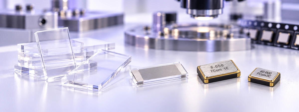
SAW devices use a piezoelectric material and patterned electrodes to couple electrical signals with acoustic motion near the material’s surface. Electrode geometry, material properties and device architecture shape the frequency response. This enables compact frequency-selective devices for communication systems. [1]
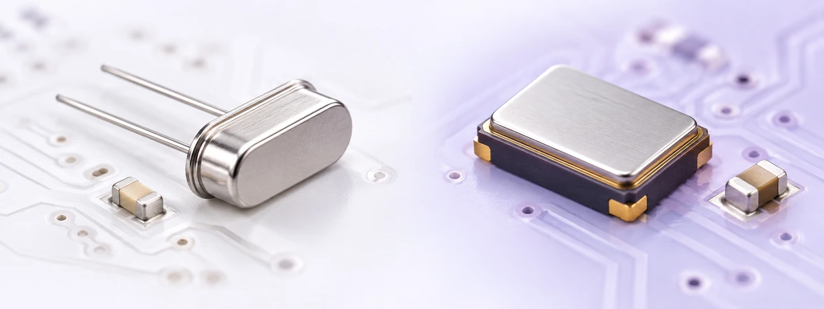
A SAW filter and a SAW resonator are related devices with different circuit roles. A filter is selected for its transmission response across a frequency band; a resonator provides a resonance that can be used in a suitable circuit. Neither name alone specifies a complete oscillator or a source of power gain.
Read the response before comparing parts
Identify the wanted band, the transition regions and the frequencies requiring rejection. Then check amplitude variation and, where relevant to the signal, phase or group-delay behavior. A single center-frequency label cannot describe that complete response.
Before moving on: sketch the signal path and mark the wanted frequency interval and principal interferers. State whether the filter operates at RF or IF.
2. Selection: turn system needs into specifications
Start with a requirements sheet rather than a package or frequency label. Write down the conditions under which each limit must hold, and compare guaranteed specifications separately from typical curves.
| Parameter | What to specify or verify |
|---|---|
| Frequency coverage | Wanted lower and upper frequencies, including the system’s required margins. |
| Bandwidth | The attenuation threshold and reference level used to define the band edges. |
| Insertion loss and ripple | Maximum loss and allowed variation across the required passband. |
| Stopband attenuation | Minimum rejection at specified frequencies or frequency intervals. |
| Port conditions | Source/load impedance, balanced or unbalanced topology, and required matching network. |
| Environment and power | Operating temperature and permitted input-power conditions for the exact part. |
| Mechanical integration | Package, pin functions, land pattern and assembly requirements. |
Bandwidth values are comparable only when their definitions agree. For example, a bandwidth measured 3 dB below the transmission peak is different from a frequency interval meeting an absolute insertion-loss limit. Check the datasheet’s reference rather than assuming every “3 dB” label means the same thing. [2]
Include matching components in the loss budget. Real inductors and capacitors introduce loss, and their Q and tolerances can affect the assembled response. A nominal component value alone is insufficient for choosing an RF matching part. [3]
Before moving on: prepare a candidate list with the same specification fields, units and test conditions. Flag any requirement that lacks supporting data.
3. Measurement: evaluate transmission and reflection
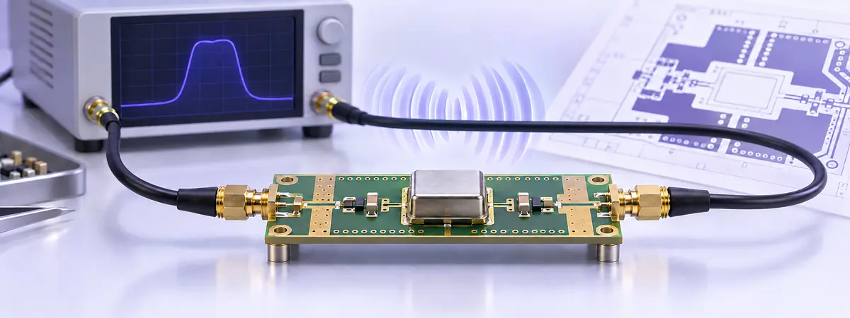
A vector network analyzer (VNA) characterizes transmission and reflection. For a conventional single-ended two-port setup, S21 describes forward transmission, while S11 and S22 describe input and output reflection. Balanced interfaces require an appropriate connection and mixed-mode measurement approach. [4]
- Define the measurement boundary. Decide whether the result should include the connectors, PCB fixture and matching network or represent the device after fixture removal.
- Match the specified port conditions. Confirm the filter topology and reference impedances. A VNA with 50 Ω ports does not make every filter a directly matched 50 Ω device.
- Calibrate the required ports. Use the instrument’s appropriate calibration procedure and account for connections between the calibration plane and the device.
- Capture the complete response. Check passband loss, ripple, band edges and required stopband intervals; review reflection alongside transmission.
- Record the setup. Save the fixture revision, matching values, temperature, source power, frequency span, point count, IF bandwidth and calibration information.
Group delay describes the rate of change of transmission phase with frequency. Its displayed value depends on the measurement aperture and noise. Record the aperture when comparing traces. A delay-only port extension also does not remove arbitrary fixture mismatch; more complete fixture characterization may be necessary. [5]
Before moving on: create a reference measurement that another engineer can reproduce. Keep the raw data as well as annotated plots.
4. PCB layout: preserve performance on the board
Use the exact device’s recommended footprint and reference layout as the starting point. Treat the filter, matching network, ground connections and adjacent routing as one RF assembly.
- Plan the transmission-line geometry from the actual PCB stackup and required impedance.
- Keep matching parts close to the relevant pins and provide short RF return paths.
- Review input-to-output coupling and avoid unnecessary parallel routing around the filter.
- Follow the manufacturer’s ground-pin and keep-out guidance; verify every pin against the package drawing.
- Reserve practical access for measurement and matching adjustments during prototype evaluation.
Integrate ESD protection into the RF review
Where protection is required, review both its RF loading and its discharge-current path. Place the protection device close to the external entry point, minimize the inductance to its return, and avoid a long branch between the signal trace and protection pin. Keep exposed discharge paths away from sensitive unprotected routing. [6]
Measure the populated board with its intended protection and matching components. If the response differs from the reference result, compare the measurement boundary, assembly and layout before attributing the change to the filter itself.
Complete the loop: return to the measurement stage after layout, matching or protection changes. Document the final configuration used for acceptance.
Frequently asked questions
Which section should I read first?
For a new design, follow the four stages in order. If you already have hardware with an unexpected response, start with measurement, confirm the test conditions, and then review PCB layout.
Can I select a filter by center frequency alone?
No. Use the selection checklist to define the full passband, rejection requirements, interfaces and operating conditions. Request clarification wherever the datasheet does not cover your acceptance criteria.
Why can two measurements of the same filter differ?
Different port impedances, matching networks, reference planes and fixture corrections can produce different results. Align those conditions before comparing traces; for group delay, align the aperture as well.
Discuss your SAW filter requirements with FCom
Send your frequency plan, required bandwidth definition, loss and rejection limits, source/load impedances, operating temperature and package constraints to FCom@fujicrystal.com. For measurement questions, include the schematic, fixture details and measured traces so the discussion can focus on the relevant conditions.
Technical references
- Murata — SAW device technology and operating principles.
- Keysight — Filter measurements: bandwidth, insertion loss and ripple.
- Murata — SAW filter matching and inductor loss.
- Keysight — Measuring an unbalanced-to-balanced SAW bandpass filter.
- Keysight — Group delay, electrical delay and port extension.
- Texas Instruments — ESD Protection Layout Guide (PDF).