Oscillator design
A practical guide to load capacitance, startup margin, crystal drive and PCB layout.
FCom Fuji Crystal · Technical Guide
A reliable Pierce oscillator needs the correct crystal load, enough gain to start, and controlled drive during operation. Check these together on the final PCB: a capacitor or resistor change can improve one condition while weakening another.
How the Pierce circuit works
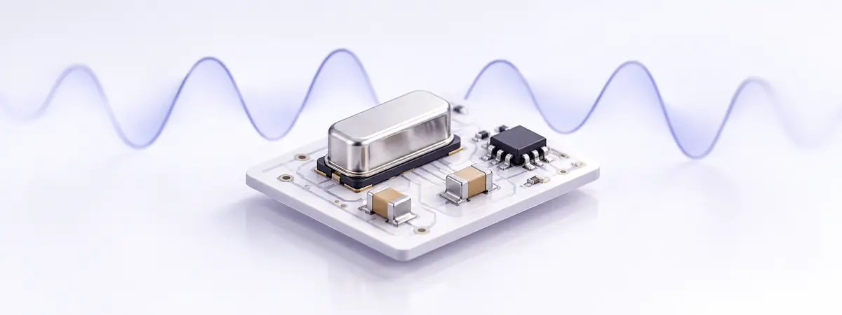
A typical Pierce oscillator combines an inverting amplifier, a passive quartz crystal and two load capacitors. The amplifier supplies energy, while the crystal and capacitive network select the operating frequency and establish the feedback phase.
A feedback resistor, Rf, establishes DC bias around the amplifier. A separate series resistor, Rs, may limit crystal drive. Microcontrollers can integrate biasing, loading or amplitude control, so use the device’s recommended circuit before adding external components.
Barkhausen: startup and steady state
In a simplified feedback model, startup requires small-signal loop gain greater than unity at a frequency with a total phase shift of 0° modulo 360°. As amplitude grows, circuit nonlinearities or amplitude control reduce the effective loop gain toward unity.[1]
The steady-state Barkhausen condition alone does not establish reliable startup. Component tolerances, supply conditions, bias and unwanted resonant modes also matter. A circuit that starts once at room temperature still needs validation across its operating range.
Choose capacitors from the specified load
The crystal’s specified load capacitance, CL, is the effective load at which its nominal frequency is defined. It is not the value of each external capacitor. For a simple two-capacitor network:
Cstray represents the effective contribution of pin, pad and trace capacitances in this approximation. It is not the crystal’s internal shunt capacitance, C0. Include programmable or integrated load capacitors using the IC manufacturer’s model; do not count them twice.[2]
Worked example
Illustrative assumptions: CL = 12 pF, effective Cstray = 2 pF, and equal external capacitors.
The check is 20 × 20 ÷ (20 + 20) + 2 = 12 pF. Treat this as an initial value, then verify frequency, startup and drive on the assembled board.
Increasing load usually lowers the operating frequency of a parallel-loaded crystal. Reducing load can improve startup margin, but shifts frequency and may increase sensitivity to small capacitance changes. Unequal capacitors require circuit-specific validation; a particular ratio is not a universal improvement.
Verify negative-resistance margin
Viewed from the crystal terminals, the active network can present a negative resistance that offsets resonator losses. Its magnitude must exceed the effective loss resistance for oscillation to grow. For margin calculations, use compatible resistance definitions and the crystal’s specified worst-case ESR.
Follow the IC vendor’s required safety factor. For the STM32/STM8 oscillators covered by ST AN2867, the stated safe thresholds are at least 5 for HSE and 3 for LSE. These are device-family guidelines, not a universal rule for all MHz or 32.768 kHz circuits.[2]
Series-resistor startup test
- Keep the actual crystal installed and add a temporary, low-parasitic resistor in series.
- Increase the added resistance in steps, restarting the oscillator from its specified off state each time.
- Record the boundary between reliable and failed startup across repeated trials and operating conditions.
- Apply the vendor’s calculation and acceptance criteria, then remove the temporary test resistor.
In the simplified boundary model, available negative-resistance magnitude is approximately the added boundary resistance plus the crystal’s effective ESR. An already-running oscillator may continue with more resistance than it can tolerate during startup; do not substitute a stop-oscillation test for a startup test.[3]
AC impedance injection is another characterization method, but requires a controlled bias point and a suitable fixture. Use the semiconductor vendor’s procedure rather than an improvised signal injection into oscillator pins.
Keep crystal drive within its rating
Drive level is power dissipated in the resonator, usually specified in microwatts. In the motional equivalent circuit:
Im,rms is RMS current through the motional branch, and Rm is its resistance. Terminal current can differ because current also flows through C0. Use the current and resistance definitions required by the chosen measurement method.
Illustrative example: 0.5 mA RMS motional current through 40 Ω dissipates 10 µW. Compare the result with the selected crystal’s rating; 10 µW is not a universal target.
Do not apply P = V2/ESR directly to the voltage measured across a parallel-loaded crystal. The crystal presents a reactive impedance. Use a documented current measurement or vendor voltage-based method that includes the circuit capacitances.
If drive is excessive, use a supported drive-strength setting or an appropriate series resistor. Recheck startup afterward. Rf controls bias and should not be treated as a general-purpose gain adjustment. Neither resistor has a universal value.
Layout and 32.768 kHz considerations
- Place the crystal and load capacitors close to the oscillator pins, with short connections and the recommended ground return.
- Keep switching supplies, RF routes and fast digital signals away from sensitive oscillator nodes.
- Follow the IC reference layout for ground copper, shielding and guard structures; added copper changes capacitance.
- Use local supply decoupling specified for the IC and control board contamination and leakage.
For 32.768 kHz tuning-fork crystals, check the particular ESR and drive limits. Do not reuse MHz crystal settings or assume that every watch crystal needs the same margin. Leakage, probe loading and long startup times deserve particular attention in low-power RTC circuits.
Troubleshooting and release checks
| Symptom | Check first | Verify after correction |
|---|---|---|
| Slow or failed startup | Clock configuration, supply ramp, ESR, loading and bias | Repeated starts and margin over voltage and temperature |
| Frequency offset | Specified load, parasitics, capacitor tolerance and measurement loading | Frequency budget and startup margin |
| Excessive crystal power | Drive setting, series resistance and measurement method | Drive limit and reliable startup together |
| Failure when probed | Probe capacitance, ground connection and test point | Operation with an appropriate measurement setup |
Prefer a buffered clock output for frequency checks. Crystal-node measurements require suitable low-capacitance probes and a loading assessment. A large waveform alone does not prove acceptable drive or startup margin.
Before release, test multiple boards across specified voltage and temperature limits, power ramps and restart modes. Include capacitor tolerances and maximum crystal ESR in the assessment. Confirm firmware timeout settings and retain the component values, measurement method and results.
Common questions
Can I copy the capacitors from a reference board?
Only after checking the same crystal specification, IC loading and PCB parasitics. Identical nominal frequency does not establish electrical compatibility.
Should I always reduce capacitance to fix startup?
No. First confirm configuration, supply and crystal compatibility. A capacitance change also shifts frequency and requires renewed validation.
Is Pierce always better than Colpitts or Clapp?
No topology guarantees the best noise or startup performance. Pierce suits many integrated crystal interfaces; choose other circuits according to their active device, resonator and application requirements.
Does a TCXO need these external load capacitors?
A packaged TCXO contains its resonator circuit. Follow its supply, output-load and control-pin requirements instead of adding a Pierce crystal network.
Discuss your crystal requirements with FCom
Share the IC part number, frequency, load capacitance, ESR limit,
drive rating and operating conditions with
FCom@fujicrystal.com
for selection support.