Clock Interfaces · Technical Guide
An HCSL crystal oscillator combines a quartz-based frequency source with a differential clock output. Choosing one requires more than matching frequency and package size: the output circuit, receiver bias, termination and jitter measurement must fit the complete clock path.
FCom Fuji Crystal · Technical Guide
1. How an HCSL oscillator works
A quartz resonator provides a frequency-selective element in an active feedback circuit. The oscillator sustains oscillation and delivers a usable clock through its output stage. A passive crystal alone cannot drive an HCSL input; it requires an oscillator circuit.
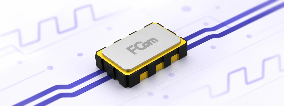
Traditional HCSL outputs steer current between complementary pins. Their external loads convert that current into voltage. The receiver detects the difference between the two signals, while common-mode voltage describes their average. Differential signaling helps reject noise shared by both lines, but layout imbalance and receiver limitations still matter.
Illustrative calculation: A 14 mA current through 50 Ω produces 0.70 V by V = IR. Ideal complementary outputs switching between 0 V and 0.70 V give a 0.35 V common-mode level and a differential waveform from −0.70 V to +0.70 V: 1.40 V peak-to-peak. These are explanatory values, not FCom product specifications. [1]
2. Driver types and termination
Traditional current-steering HCSL and low-power HCSL can serve similar receiver interfaces while needing different external circuits. Confirm the exact ordering option before placing resistors.
| Output type | Typical implementation | Design check |
|---|---|---|
| Traditional HCSL | Switched-current output with a DC return through a termination to ground on each leg. | Confirm resistor values, placement and any series damping. |
| Low-power HCSL | Often a voltage-mode or push-pull driver with integrated source termination. | Check supported line impedance and whether external termination is required. |
For example, TI specifies 50 Ω to ground near each LMK00334 output, with optional series resistors to control overshoot. This is a device-specific circuit, not a universal instruction to terminate every differential clock at its source. [2]
Renesas describes low-power HCSL devices with integrated termination options for 85 Ω or 100 Ω differential environments. Do not automatically add traditional HCSL shunt resistors to such outputs: the extra load may change their signal levels. Follow both the driver and receiver documentation. [3]
3. Receiver compatibility and coupling
HCSL, LVDS and LVPECL are different electrical interfaces. A shared differential pin arrangement does not establish compatibility. Compare input common-mode range, differential swing, absolute input limits, slew rate and internal termination. [1]
DC coupling is appropriate when source and receiver levels are compatible. AC coupling can separate their DC bias levels, but the receiver then needs its specified bias arrangement. For traditional HCSL, retain the required DC path from the driver to ground; a series capacitor must not interrupt that path. [2]
Document which resistors and bias circuits are already inside each device. Check the entire network before adding a 100 Ω resistor across the receiver inputs or copying a schematic from another output standard.
4. PCIe clock architecture and jitter
A 100 MHz HCSL reference is common in PCIe systems, but the interface name alone does not qualify an oscillator for a particular generation. Start by identifying how the two link partners obtain their clocks. [4]
- Common Clock: Both ends share a reference; the distribution path and clock correlation affect the jitter analysis.
- SRNS: Separate Reference No Spread uses independent references without spread-spectrum modulation.
- SRIS: Separate Reference Independent Spread supports independent references with spread-spectrum operation, subject to endpoint support.
Apply the relevant specification revision, generation and architecture. A generic RMS phase-jitter value integrated over 12 kHz to 20 MHz does not by itself establish PCIe compliance. PCIe assessment uses defined filtering that reflects clock and data-recovery behavior; different architectures require different treatment. [5]
Include the oscillator, buffers and distribution channel in the timing assessment. Request the measurement method, filter settings, operating conditions and applicable limits with any compliance claim. Preserve the distinction between an oscillator’s total output jitter and a buffer’s additive jitter.
Spread-spectrum clocking (SSC) intentionally modulates frequency. It requires an SSC-capable source and compatible system configuration; HCSL does not imply SSC capability. Record spread depth, modulation rate and operating mode, and verify that every clock-path component supports the selected configuration. [4]
5. PCB layout and power integrity
Fast clock edges make interconnect geometry important even when the fundamental clock frequency appears modest. Route the pair with controlled impedance and matched electrical delay. Keep a continuous reference plane, minimize stubs and unnecessary vias, and avoid routing across plane splits.
Place termination components where the selected driver topology requires them. Keep both legs geometrically similar, including pads, vias and test access. Validate the impedance against the PCB stack-up instead of treating trace width alone as sufficient.
Place the specified bypass capacitors close to the supply pins with short ground connections. Supply disturbances can degrade phase noise and jitter. If additional RC or LC filtering is needed, check voltage drop, startup behavior and possible filter resonance before adopting it. Component values must suit the selected oscillator. [6]
6. Selection and bench validation
Prepare a requirements sheet before requesting a part recommendation:
- Output frequency, supply range, operating temperature and frequency-stability definition.
- Driver type, receiver part number, coupling and termination circuit.
- Package, pin assignment, enable function and startup requirements.
- Jitter metric, measurement bandwidth or filters, and required system margin.
- PCIe generation, clock architecture and SSC settings, where applicable.
On the prototype, inspect both single-ended outputs and the differential waveform at the receiving end using suitable probes. Check common mode, swing, overshoot, ringing and duty cycle. Account for probe loading; attaching a 50 Ω instrument input can change the intended termination.
Measure jitter with the agreed method and repeat key checks across the required supply and temperature range. A clean-looking waveform or a successfully trained link is useful evidence, but neither replaces the required electrical and timing evaluation.
7. Frequently asked questions
Can I replace an LVDS oscillator with HCSL?
Only after checking levels, bias and termination. Matching frequency and footprint is insufficient; a conversion network or compatible receiver may be needed.
Does every HCSL output need two external 50 Ω resistors?
No. Traditional drivers commonly require ground-referenced loads, while low-power implementations may integrate termination. Use the exact device schematic.
Does lower ppm mean lower jitter?
No. Frequency accuracy describes deviation from nominal frequency under stated conditions. Jitter describes timing variation. Specify and verify both separately.
Is an HCSL oscillator automatically suitable for PCIe?
No. Suitability depends on electrical limits, the intended PCIe generation, clock architecture, SSC configuration and the required jitter assessment.
Technical references
The following manufacturer resources explain interface and measurement principles. Their device-specific circuits and performance data apply to the stated devices.
- SiTime: AN10029 — Output Terminations for Differential Oscillators.
- Texas Instruments: LMK00334 datasheet, termination and coupling guidance.
- Renesas: PCI Express Clock Overview, low-power HCSL and integrated termination.
- Renesas: PCIe Gen 5 and 6 CC/SRIS/SRNS Clocking with VersaClock 7 Devices.
- Renesas: PCI Express Common Clock Jitter Model and Transfer Functions.
- SiTime: AN10006 — Best Design and Layout Practices.