Clocking Fundamentals
A CMOS crystal oscillator supplies a digital clock to an electronic circuit. Choosing the right device means matching its frequency and electrical interface to the receiving IC, then checking timing accuracy, power consumption and operating conditions.
FCom Fuji Crystal · Technical Guide
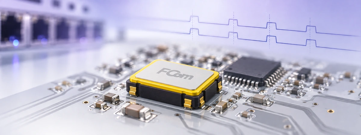
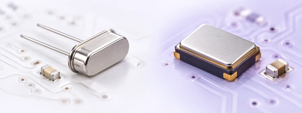
What is a CMOS crystal oscillator? It is an active timing device that combines a quartz resonator, sustaining circuitry and a CMOS output stage. After power is applied and startup is complete, it delivers a periodic logic-level clock. A passive quartz crystal requires an external oscillator circuit.
How does a CMOS crystal oscillator work?
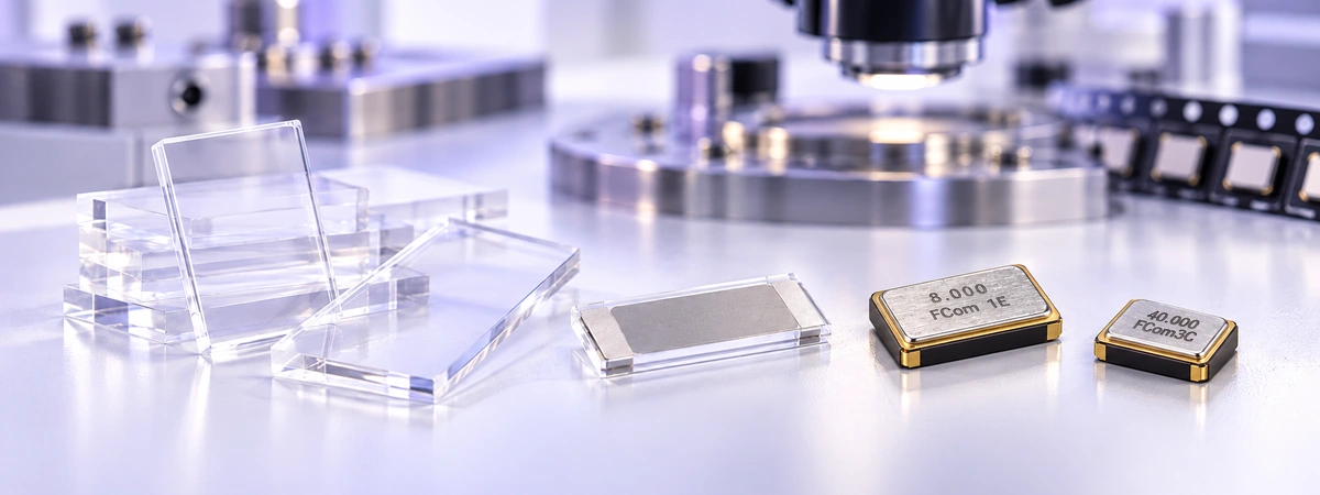
Quartz couples electrical energy and mechanical vibration through the piezoelectric effect. In an oscillator, the resonator forms part of a feedback network. The active circuit supplies energy to overcome losses and sustain oscillation; the crystal provides a frequency-selective reference. [1]
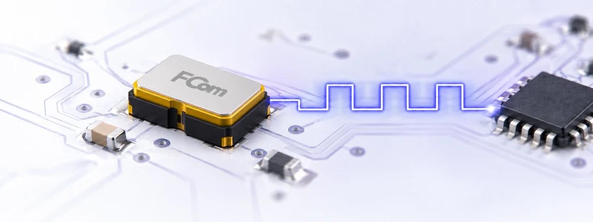
An output buffer converts the internal signal into a clock suitable for a digital input. Some devices also include a PLL or divider, so the output frequency is not necessarily the crystal’s own resonant frequency. The actual architecture and available functions depend on the device. [2]
CMOS, LVCMOS and oscillator types
CMOS means complementary metal-oxide-semiconductor. In oscillator specifications, CMOS or LVCMOS commonly identifies the output interface. LVCMOS refers to low-voltage CMOS signaling. Neither label alone specifies frequency stability, jitter or temperature compensation.
| Term | Meaning | Selection implication |
|---|---|---|
| Quartz crystal | Passive resonator. | Requires a compatible external oscillator circuit. |
| XO / SPXO | Packaged oscillator without temperature compensation or oven control. | Check its specified frequency stability. |
| TCXO | Temperature-compensated crystal oscillator. | Used when temperature-related frequency error needs tighter control. |
| VCXO | Crystal oscillator with voltage-controlled frequency adjustment. | Check tuning range and control-voltage requirements. |
| CMOS / LVCMOS | Single-ended logic output referenced to ground. | Match output levels and load to the receiver. |
| LVDS / LVPECL | Differential output interfaces. | Require compatible receivers and appropriate termination. |
A TCXO or VCXO can have a CMOS output. Conversely, a CMOS-output XO does not automatically include temperature compensation. Output interface and frequency-control method must be checked separately. [2] [3]
Benefits and typical applications
A packaged oscillator removes the need to design the crystal’s sustaining circuit on the PCB. Compact SMD packages simplify placement, while a compatible CMOS output connects to a digital clock input.
Typical uses include MCU and FPGA reference clocks, consumer electronics, communication equipment and industrial controllers. Portable designs may prioritize current consumption; communication and measurement systems may require tighter jitter or frequency-error limits. Automotive designs also require the relevant qualification and environmental ratings.
Low power, low phase noise, fast startup and long service life are device-specific characteristics. They should be supported by the selected part’s documentation rather than inferred from the CMOS label.
How to select a CMOS crystal oscillator
Start with the receiving IC’s clock-input requirements and use them to review the oscillator datasheet.
- Frequency: confirm the required clock rate and permitted deviation.
- Supply and logic levels: compare guaranteed output-high and output-low voltages with the receiver’s thresholds and absolute maximum ratings.
- Frequency accuracy: identify whether the specification includes initial tolerance, temperature, supply variation, output loading and aging.
- Output load: include receiver input capacitance, PCB traces and other parasitic capacitance.
- Waveform: check duty cycle and rise/fall times at the specified load and measurement thresholds.
- Jitter: match the required metric. Integrated phase-jitter values are comparable only with compatible integration bands and test conditions.
- Power and control: check loaded current, startup time, enable behavior and any standby function.
- Mechanical and environmental fit: verify package height, footprint, pin assignment, operating temperature and assembly requirements.
Terminology and test conditions matter as much as the headline numbers. [3]
Frequency accuracy and timing error
Frequency error describes deviation from the nominal clock rate. Jitter describes short-term variation in edge timing. A low-jitter clock can still have a frequency offset; one specification does not replace the other.
Illustrative calculation
Frequency error (Hz) = nominal frequency (Hz) × error (ppm) ÷ 1,000,000
At 25 MHz, ±20 ppm corresponds to ±500 Hz. If a constant 20 ppm offset drives an uncorrected time counter, the magnitude of accumulated error after one day is 86,400 × 20 ÷ 1,000,000 = 1.728 seconds.
This is a mathematical example, not a FCom product specification. Actual time error depends on changing operating conditions and any system correction.
Build the error budget from the conditions the system will encounter. Avoid adding temperature or aging limits twice if they are already included in a total stability specification.
PCB integration and power considerations
- Follow the selected device’s supply-decoupling guidance and keep the capacitor connection loop short.
- Keep the clock route short with a continuous ground return. Avoid unnecessary stubs and excessive fanout.
- Evaluate signal integrity using edge speed and interconnect length; clock frequency alone does not determine reflection risk.
- Check the waveform at the receiver with a suitable low-capacitance probe. Include probe loading when interpreting measurements.
- Set the receiving IC to the appropriate external-clock mode and observe startup or clock-valid requirements.
Charging a CMOS output load consumes current. As a first-order estimate for a full-swing clock, the load-related power is P ≈ Cload × VDD2 × f. Internal oscillator consumption is additional. Increasing capacitance, voltage or frequency therefore affects the power budget. [4]
Frequently asked questions
Can a CMOS oscillator directly replace a passive crystal?
No. Their connections and functions differ. A replacement requires a suitable external-clock input, power, correct logic levels and the clock configuration specified by the receiving IC.
Does a CMOS crystal oscillator need external load capacitors?
A packaged oscillator normally contains its resonator network. Do not add the two crystal-loading capacitors used in a discrete crystal circuit by default. Supply decoupling and any output termination must follow the oscillator’s application guidance.
Can a 3.3 V oscillator drive a 1.8 V clock input?
Only if the receiver explicitly supports those input levels. Otherwise, select a compatible oscillator output or a suitable clock-level translator. Matching frequency alone is insufficient.
Are output enable and standby the same?
Not necessarily. Output enable may disable only the buffer, while standby may stop additional circuitry to save power. Current, output state and recovery time depend on the part. [4]
When should I consider a TCXO?
Consider a TCXO when a standard XO cannot meet the system’s frequency-error budget over temperature. Confirm that its output interface, power and startup behavior also suit the design.
Discuss your clock requirements with FCom
Explore the FCom CMOS oscillator family, or email FCom@fujicrystal.com with your required frequency, supply voltage, receiver interface, output load, stability, temperature range and package constraints.
Technical references
- Epson: Basic Knowledge of Crystal Unit — resonator behavior and sustaining circuits.
- Epson: Crystal Oscillators — packaged oscillators and functional categories.
- SiTime: Timing Terminology Glossary — output interfaces and timing definitions.
- SiTime: Oscillator FAQs — CMOS load current and control functions. Device-specific examples do not define FCom product ratings.