FCom Fuji Crystal · Technical Guide
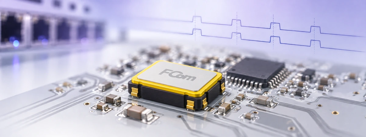
A clipped sine wave oscillator supplies a periodic reference signal whose peaks are limited rather than forming a pure sinusoid. This output is common in compact timing devices, including TCXOs, where a compatible receiver can accept a modest signal swing. Selecting one requires checking the complete electrical interface, not just the waveform name.
Key point: clipped sine describes an output waveform. It does not specify frequency accuracy, temperature compensation, supply voltage or CMOS compatibility. Those characteristics must be read separately in the oscillator and receiver datasheets.
What clipped sine means
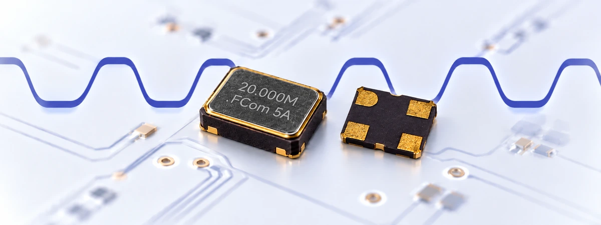
Amplitude limiting flattens or compresses portions of a sine-like waveform near its peaks. The actual shape depends on the output circuit and load. Clipping introduces harmonics, so a clipped sine wave is not a distortion-free sinusoid. It also does not automatically meet the voltage levels and edge specifications of a digital square-wave output.
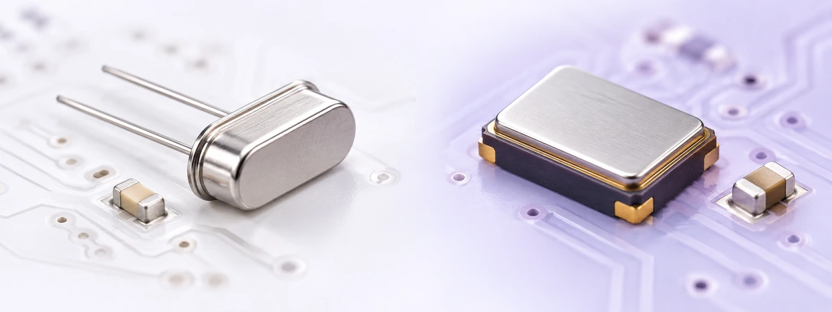
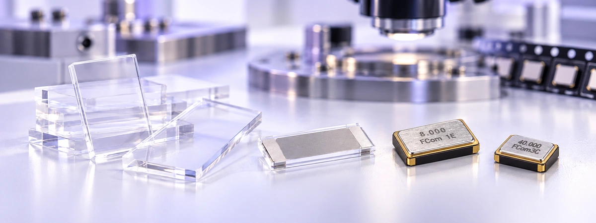
In a quartz oscillator, the resonator and sustaining circuit establish the oscillation; the output stage presents a usable signal to the external circuit. A packaged oscillator normally provides a specified waveform. It is not a laboratory waveform generator with a user-adjustable clipping threshold.
TCXO means temperature-compensated crystal oscillator, while VCTCXO adds voltage-controlled frequency adjustment. Output format and frequency-control function are separate choices. Clipped sine output also exists in non-quartz timing technologies; SiTime, for example, documents it as an option on a MEMS oscillator. [5]
Clipped sine, sine and CMOS compared
| Output | Typical description | Main checks |
|---|---|---|
| Clipped sine | Sine-like signal with limited peaks. | Peak-to-peak voltage, load, coupling and receiver sensitivity. |
| Sine wave | Analog periodic signal with rounded peaks. | Amplitude or power, specified impedance and harmonic content. |
| CMOS / LVCMOS | Logic waveform with specified high and low levels. | Logic thresholds, capacitive load, duty cycle and edge rates. |
Clipped sine can reduce output-stage power compared with a full digital driver in some oscillator designs. Any advantage must be evaluated with the required receiver or conversion buffer included. The output label alone does not guarantee lower system power, better phase noise or lower emissions. [1]
Amplitude and output loading
A voltage specification is meaningful only with its test conditions. For clipped sine outputs, look for minimum peak-to-peak voltage, supply range, temperature and the specified resistive and capacitive load.
For example, Epson’s TG-5511CA family documentation includes a clipped-sine option characterized with a nominal 10 kΩ resistance in parallel with 10 pF capacitance. Its test circuit counts probe capacitance within the load. These are manufacturer-specific conditions, not universal values or FCom product specifications. [2]
The oscillator sees the combined receiver, PCB, fixture and probe loading. A “10 pF load” does not necessarily mean adding a separate 10 pF capacitor. Likewise, connecting a high-impedance output directly to a 50 Ω instrument input can substantially reduce the signal. Use the documented measurement arrangement.
Vpp = Vmax − Vmin
Illustrative example: a 0.8 V peak-to-peak signal centered at 0.9 V spans approximately 0.5–1.3 V. That range does not establish CMOS compatibility; compare it with the receiver’s actual input specifications.
AC coupling and receiver compatibility
Many clipped-sine interfaces use a series DC-blocking capacitor. This lets the source and receiver operate at different DC bias levels. The receiving input must have an appropriate internal or external bias path; a coupling capacitor alone does not establish its operating point.
Follow the recommendations for both devices. CTS specifies a coupling arrangement for its covered TCXO families, but the capacitor value must not be assumed suitable for every oscillator and receiver. Check whether coupling is already integrated, along with input impedance and startup settling. [1]
Before connecting the clock, confirm:
- The receiver explicitly accepts the available waveform and frequency.
- Signal swing and bias satisfy its operating limits across temperature and supply variation.
- Input slew rate, loading and absolute maximum ratings are respected.
If conversion to CMOS is required, use a suitable clock buffer or conditioning circuit. Evaluate its input sensitivity, biasing, output levels and added noise. An arbitrary logic inverter is not a universal converter. [3]
Phase noise, jitter and signal edges
Clipping harmonics and phase noise are different phenomena. Harmonics occur at integer multiples of the fundamental; phase noise describes fluctuations around the carrier, commonly specified in dBc/Hz at stated offsets. A visibly clean waveform does not prove low phase noise.
Integrated RMS phase jitter depends on the integration bandwidth and carrier frequency. Compare results only under equivalent conditions, and evaluate noise through the complete clock path. Analog Devices’ MT-008 explains the relationship between phase-noise power and time jitter. [4]
Receiver performance also depends on signal slope near the switching threshold. A compatible buffer can improve the transition presented to a downstream device, but contributes noise of its own. TI discusses how amplitude, slew rate and bias affect sine-to-square conversion. [3]
Applications and selection checklist
Potential uses include reference clocks for compatible RF synthesizers, wireless receivers, GNSS systems and timing circuits. Suitability follows the receiving chipset’s requirements. A clipped-sine timing source is not, by itself, an audio effects generator or a programmable motor-control waveform source.
- Frequency: nominal value, initial tolerance, temperature stability and aging interval.
- Output: minimum amplitude, permitted load, coupling and receiver requirements.
- Noise: phase noise at relevant offsets and jitter over a stated bandwidth.
- Power: supply tolerance, operating current and standby behavior where available.
- Control: startup time, enable function and any specified frequency-tuning range.
- Integration: package, pinout, assembly requirements and operating environment.
Do not transfer specifications between output variants sharing a product-family name. Confirm the complete ordering code and its applicable electrical table.
Board layout and measurement
Place recommended supply decoupling close to the oscillator, maintain a short return path and keep sensitive clock and voltage-control traces away from switching nodes. CTS highlights supply filtering, load matching and control-pin noise as practical TCXO design considerations. [1]
Measure amplitude at the receiver with a low-capacitance probe and account for its loading. SiTime’s clipped-sine test diagrams explicitly include probe and fixture contributions and use a buffer for phase-noise measurement. [5] Verify startup, frequency, receiver operation and noise under the intended supply and temperature conditions.
Frequently asked questions
Can clipped sine drive a CMOS input directly?
Only when the receiver’s voltage, bias and transition requirements are met. Otherwise, use a compatible conversion stage or select an oscillator with the required logic output.
Does every clipped-sine oscillator need an external coupling capacitor?
No single rule covers every device. Check both datasheets for internal coupling, output bias and the recommended connection circuit.
Is 10 kΩ in parallel with 10 pF a universal load?
No. It is a common specified condition for certain devices. Use the exact limits for the selected part and include board and measurement loading.
Does clipped sine guarantee better frequency stability?
No. Stability depends on the oscillator design and stated operating conditions. Output waveform, temperature compensation and frequency accuracy are separate specifications.
Discuss your clock interface with FCom. Send your required frequency, supply voltage, temperature range, stability, minimum signal amplitude, load and receiver part number to FCom@fujicrystal.com. Include phase-noise or jitter requirements and the proposed coupling circuit when available.
Technical references
- CTS. Small Package TCXO User Guide. PDF.
- Epson. TG-5511CA documentation. See the included family specifications and clipped-sine test circuit. PDF.
- Texas Instruments. SNAA411: Sine to Square Wave Conversion Using Clock Buffers. PDF.
- Analog Devices. MT-008: Converting Oscillator Phase Noise to Time Jitter. PDF.
- SiTime. SiT5156 datasheet. Output options and clipped-sine measurement circuits. PDF.