RF & IF Filtering · Technical Guide
A crystal filter selects a frequency band using quartz resonators. For engineers choosing a filter for an intermediate-frequency (IF) signal path, the key task is to preserve the wanted signal while rejecting interference under the actual circuit conditions.
FCom Fuji Crystal · Technical Guide
1. What a crystal filter does
A quartz resonator converts electrical excitation into mechanical vibration through the piezoelectric effect. Its sharply frequency-dependent impedance enables selective filtering. Commercial crystal filters are commonly bandpass devices used for narrowband signal selection. [1]
A passive crystal filter processes an incoming signal. It does not generate a clock like an active oscillator, amplify the wanted signal or automatically correct an oscillator’s frequency drift. It can attenuate interference outside its passband, but cannot separate wanted and unwanted signals that occupy the same frequencies.
Typical design contexts include communication receivers and narrowband IF stages. Choose the technology from the required frequency response: a crystal filter is not a general substitute for an audio equalizer, broadband RF filter or digital signal-processing function.
2. Construction and design choices
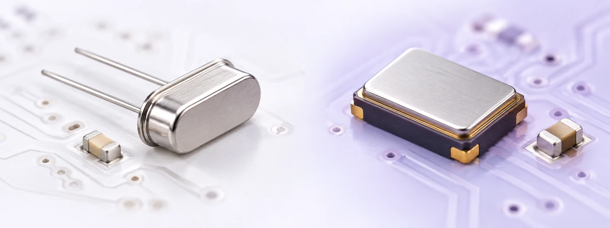
Discrete crystal filters use individual resonators with coupling components. Ladder and lattice networks are examples. Monolithic crystal filters (MCFs) use coupled resonant regions on a quartz blank. Multiple sections can form a higher-order response. [1]
More poles can provide steeper rejection skirts, but pole count alone does not describe loss, ripple or phase behavior. Chebyshev, Butterworth and linear-phase approaches make different compromises. Specify the needed response instead of assuming the highest pole count is always best.
For a discrete design, characterize resonator frequency, equivalent-circuit parameters and losses before synthesis. Crystals with the same marked frequency are not necessarily matched filter elements. Simulate with realistic source/load impedances and component tolerances, then verify the assembled network.
Crystal resonator Q helps make narrow bandwidths practical, but the achievable response also depends on coupling, capacitance ratio and circuit losses. It is not set by resonator Q alone. [2]
3. Read the specifications correctly
Compare filters using the same definitions and test conditions. A 3 dB bandwidth, a 6 dB bandwidth and a ripple-defined passband are different quantities. A bandwidth written as ±7.5 kHz describes a 15 kHz total span around the stated center. [3]
| Parameter | What to define |
|---|---|
| Center frequency | Nominal value, permitted offset and operating conditions. |
| Passband | Required frequency interval and attenuation or ripple criterion. |
| Insertion loss | Maximum allowed loss and whether evaluated at center, minimum-loss point or across the useful band. |
| Ripple | Maximum variation over an explicitly defined frequency interval. |
| Rejection | Minimum attenuation at stated offsets or throughout stated bands; identify the reference level. |
| Group delay | Allowed delay variation over the modulation bandwidth. |
| Termination | Source/load resistance, shunt capacitance and required coupling components. |
Allow passband margin for signal-frequency error and filter drift. Narrowing the bandwidth too far can remove modulation sidebands. Group-delay variation can also distort a modulated signal even when its amplitude response looks acceptable. [3]
Shape-factor example: If BW6 dB = 12 kHz and BW60 dB = 30 kHz, then SF60/6 = 30/12 = 2.5. Both bandwidths must use the same attenuation reference. A smaller ratio indicates steeper skirts at those levels; it does not describe every stopband feature. This is an illustrative calculation, not FCom product data. [4]
Check spurious-response limits separately. A deep rejection value at one offset does not guarantee equally strong attenuation everywhere outside the passband.
4. Match the source and load
Do not assume a crystal filter is a 50 Ω component. Specifications often define termination as resistance in parallel with capacitance. NDK’s catalog, for example, lists model-specific R // C terminations and distinguishes filters that need external coupling capacitors from versions with coupling built in. [5]
Account for the impedance presented by the driving and receiving circuits, matching networks and PCB parasitics. Confirm whether the specified capacitance represents the total required at the terminals before choosing external capacitors. Copying only a resistor value can leave the actual termination incorrect.
Use the manufacturer’s circuit to connect paired filter sections, including their orientation and coupling components. Keep matched pairs together where required. A replacement must match the electrical network and pin assignment as well as frequency and package. [3]
5. PCB, signal level and environment
Keep input and output paths separated to reduce unwanted feedthrough. Follow case-ground and pin instructions, use short connections around matching components, and consider shielding where high rejection is required. Parasitic coupling can limit measured rejection even when the filter itself performs correctly.
Verify the rated input level and linearity under expected wanted-signal and blocker conditions. Crystal filters can exhibit drive-level dependence and intermodulation; passive construction does not imply suitability for a transmitter’s high-power output. [4]
Check operating and storage temperatures separately, plus soldering conditions and any required vibration or shock rating. Evaluate frequency drift and response changes over the specified environment. Do not infer these limits from package appearance or from another filter in the same family.
6. Measure and validate the design
Use a calibrated vector network analyzer with a fixture that presents the specified source/load conditions. Document the calibration reference plane and whether matching-network loss is included. A bare filter connected directly to 50 Ω ports may not reproduce its specified response. [2]
- Resolve the passband: Use a narrow span and sufficient frequency points to identify the required band edges and ripple.
- Apply the right threshold: For a peak-relative 3 dB bandwidth, find points 3 dB below peak transmission. If the peak is −2 dB, the threshold is −5 dB, not −3 dB. [6]
- Inspect the wider stopband: Check every specified rejection interval and possible spurious responses. Distinguish actual response from fixture leakage or the instrument floor.
- Measure phase where needed: Record group-delay variation across the useful band and state the measurement aperture. Changing the aperture changes the detail and noise in the result. [7]
- Repeat critical conditions: Check required temperatures and input levels, staying within the device ratings.
Save response plots, test settings, fixture details, matching values and sample identification. These records make supplier comparisons and later failure analysis more useful.
7. Prepare a selection request
Provide the center frequency, usable bandwidth, ripple, loss budget, rejection mask, termination, package and environmental limits. Add group-delay and linearity requirements where the modulation or blocker environment demands them. For a replacement, include the existing datasheet and circuit.
Terms such as “original” or “in-line” do not replace electrical specifications. Confirm the manufacturer, exact part number, traceability and drawing instead of treating those descriptions as a performance grade.
8. Frequently asked questions
Is a crystal filter the same as a crystal oscillator?
No. A passive filter selects frequencies from an applied signal. An oscillator uses an active circuit to generate a periodic output.
Is the narrowest filter always the best choice?
No. Its useful passband must preserve the modulation and accommodate frequency errors. Excessively narrow filtering can distort the wanted signal.
Can a SAW filter replace a crystal filter directly?
Only after checking the complete response, impedances, signal levels and pinout. The technologies overlap in some applications but are not automatically interchangeable.
Why does the measured response differ from the datasheet?
Check termination, coupling capacitance, fixture calibration, frequency resolution, input level and temperature. Also confirm that bandwidth and attenuation use the same definitions.
Technical references
These manufacturer resources support the design principles discussed here. Product-specific values apply to the devices identified in each source.
- KVG: Quartz Filter Technology.
- NDK: Crystal Filter Terminology and Application Notes (PDF).
- TechPoint Golledge: Specifying Crystal Filters.
- ECS: Filter Application Notes (PDF).
- NDK: Crystal Filter Catalog (PDF).
- Keysight: Filter Measurements.
- Keysight: Group Delay Format.