
FSF-5050 Series · RF Through Device
40–1040 MHz RF Through Device
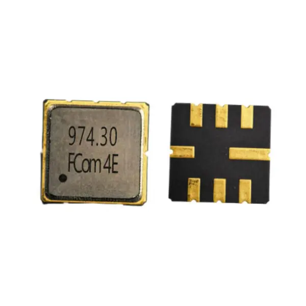
FSF-5050-974M3
A through-path component for broadband RF connections and test signal paths. Review the stated through range, insertion loss and ripple for your interface.
Key Features
Select for the Required RF Through Path
Through Range
40–1040 MHz
The stated through range. A 3 dB bandwidth and narrowband selectivity are not specified.
Insertion Loss
0.7 dB typ.
1.0 dB maximum in the electrical table. Confirm the applicable test conditions for your design.
Passband Ripple
0.6 dB typ.
1.0 dB maximum over 40–1040 MHz. Preserve this frequency interval when evaluating the limit.
Interpreting 974.3 MHz: the electrical table lists this value as fc in the typical column. It does not define a narrowband passband or a rejection characteristic. The supplied sheet describes RF through operation.
Electrical Specifications
Six Key Selection Parameters
The stated through range is 40–1040 MHz. Values below follow the supplied FCom sheet; typical values are not guaranteed limits.
Scroll horizontally to view all columns.
| Parameter | Min. | Typ. | Max. | Unit | Definition / condition |
|---|---|---|---|---|---|
| Center frequency, fc | — | 974.3 | — | MHz | As listed; not a narrowband passband definition |
| Insertion loss, IL | — | 0.7 | 1.0 | dB | Measurement frequency interval not separately stated for this row |
| Passband ripple | — | 0.6 | 1.0 | dB | 40–1040 MHz |
| 3 dB bandwidth | — | — | — | MHz | Not specified; distinct from the through range |
| Operating temperature | −30 | — | +60 | °C | Operating range |
| Storage temperature | −40 | — | +85 | °C | Storage range |
“—” means no value is specified, not zero. Source and load test terminations are 50 Ω. Electrical measurement temperature and device input/output impedance are not separately specified. The operating range is not a statement of the electrical measurement temperature. Refer to the datasheet for the complete supplied information.
Typical Applications
Broadband Connections and RF Test Paths
Broadband RF Connections
Evaluate a through connection within the stated 40–1040 MHz range. Check insertion loss and ripple against the requirements of the connected RF stages.
RF Test Signal Paths
Consider the component in a test fixture or instrument RF path requiring through transmission. Define source/load terminations and measurement reference planes.
Through-Path Evaluation
Assess an RF connection on the intended PCB using the listed pin assignment. Verify response over the frequency range your application actually uses.
Integration Notes
Reproduce the Relevant Test Conditions
Source and Load
The reference uses 50 Ω source and load terminations. These are test-port conditions; the supplied FCom sheet does not separately specify the device’s input and output impedances.
Reference Connection
The reference circuit shows input at pin 3 and output at pin 7, with no external L/C matching components drawn. Confirm whether the intended interface needs additional matching after PCB evaluation.
Board Verification
Verify grounding, signal-pad orientation, insertion loss and ripple across the required range. Confirm any frequency-selectivity requirement separately; rejection limits are not specified.
A through range is not a 3 dB bandwidth specification. Do not infer narrowband rejection or interchangeability with another FSF-5050 device from the model name or package size.
Package & Pin Assignment
5.0 × 5.0 mm, Eight-Pad SMD Package
The listed FSF-5050-974M3 configuration uses pin 3 as input and pin 7 as output. Check the selected model’s pin functions before reusing a PCB footprint.
Confirm the applicable maximum height. The supplied FCom sheet retains a 1.5 mm maximum-height template and notes a 1.7 mm reference height. Resolve this difference and confirm drawing orientation and the PCB land pattern before layout release.
Pin functions below follow the supplied FCom sheet. Contact FCom for other pin requirements.
| Pin | Function |
|---|---|
| 3 | Input |
| 7 | Output |
| 2 | Input ground |
| 6 | Output ground |
| 1, 4, 5, 8 | Ground |
Selection and Design-In Support
Define the Through-Path Requirements
Share the intended RF frequency range, application, source/load requirements, acceptable insertion loss and ripple, and operating temperature. Include sample quantity and estimated annual volume.
Ask FCom to confirm the applicable specification, package drawing and complete ordering code. State any bandwidth or rejection requirement explicitly so it can be reviewed against the through-device function.
Engineering Questions
Frequently Asked Questions
Is FSF-5050-974M3 a narrowband 974.3 MHz filter?
The supplied FCom sheet identifies RF through operation over 40–1040 MHz. It also reproduces Fc = 974.3 MHz in the typical column of the electrical table. That entry does not establish a narrowband passband, a 3 dB bandwidth or out-of-band rejection.
Is 40–1040 MHz the 3 dB bandwidth?
No. It is the stated through range and the specified interval for passband ripple. A 3 dB bandwidth is not provided. Confirm your required through range, insertion-loss limits and ripple limits for the intended circuit.
Does the reference circuit require external matching components?
The reference circuit uses 50 Ω source and load terminations and shows no external L/C matching components. Device input and output impedances are not separately specified. Evaluate the intended interface and PCB response rather than assuming every implementation needs no matching.
Which pins carry the RF signal?
Pin 3 is input and pin 7 is output. Pin 2 is input ground, pin 6 is output ground, and pins 1, 4, 5 and 8 are ground. Confirm pad orientation against the applicable drawing before PCB release; package size alone does not establish pin compatibility.
What must be confirmed about the mechanical dimensions?
The stated package footprint is 5.0 × 5.0 mm with eight no-lead SMD pads. The FCom sheet retains a 1.5 mm maximum-height template and notes a 1.7 mm reference height. Confirm the applicable maximum height, drawing orientation and PCB land pattern with FCom before layout release.
What information should I send for selection and ordering?
Provide FSF-5050-974M3, the required through frequency range, application, source/load requirements, insertion-loss and ripple limits, operating temperature, sample quantity and estimated annual volume. Include any bandwidth or selectivity requirement, and confirm the applicable specification and full ordering code with FCom.