
FSF-5050 Series · SAW Bandpass Filter
500 & 504 MHz SAW Bandpass Filters
FSF-5050-500M · FSF-5050-504M
Two frequency options for RF/IF receiver filtering and UHF signal selection, in a 5.0 × 5.0 mm SMD package.
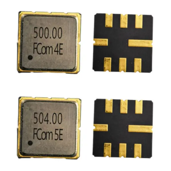
Left: marked top surface. Right: pad side. Photos do not define pin orientation.
Model Selection
Choose the Passband and Interface Conditions
The two models share a package but differ in specified passband, insertion loss, ripple, operating temperature and interface conditions. The 500 MHz model requires signal-pin confirmation before PCB layout.
Signal-pin mapping pending confirmation
FSF-5050-500M
500 MHz
Center frequency (Typ.)
- Specified passband
- 497–503 MHz
- Insertion loss over this passband
- 2.7 dB typ. / 4.7 dB max.
- Operating temperature
- −20 to +70 °C
- Interface condition
- 50 Ω source/load with external measurement matching
FSF-5050-504M
504 MHz
Center frequency (Typ.)
- Specified passband
- 500–508 MHz
- Insertion loss over this passband
- 2.5 dB typ. / 4.5 dB max.
- Operating temperature
- −40 to +85 °C
- Interface condition
- 50 Ω ∥ 0 pF input/output at 504 MHz; 50 Ω test ports
The insertion-loss and ripple values apply over different frequency intervals and interface conditions. Neither matching requirements nor interchangeability can be inferred from the shared package.
Electrical Specifications
Model-Specific Limits and Test Conditions
“—” means a value is not specified, not zero. Typical values are for design guidance. The listed frequency intervals are specified passbands, not 3 dB bandwidths.
FSF-5050-500M
The following values are reproduced from the FCom sheet for its matched measurement arrangement. The signal-pin discrepancy remains unresolved; confirm pin mapping and the applicability of this arrangement before design-in.
Scroll horizontally to view all columns.
| Parameter | Min. | Typ. | Max. | Unit | Definition / condition |
|---|---|---|---|---|---|
| Center frequency | — | 500.0 | — | MHz | FCom Typ. column |
| Specified passband | — | — | — | MHz | 497–503 MHz; insertion-loss and ripple interval |
| Insertion loss | — | 2.7 | 4.7 | dB | 497–503 MHz; with specified measurement matching |
| Amplitude ripple | — | 0.4 | 2.0 | dB | 497–503 MHz; with specified measurement matching |
| 3 dB bandwidth | — | — | — | MHz | Not specified |
| Operating temperature | −20 | — | +70 | °C | Operating range |
FSF-5050-504M
Scroll horizontally to view all columns.
| Parameter | Min. | Typ. | Max. | Unit | Definition / condition |
|---|---|---|---|---|---|
| Center frequency | — | 504.0 | — | MHz | FCom Typ. column |
| Specified passband | — | — | — | MHz | 500–508 MHz; insertion-loss and ripple interval |
| Insertion loss | — | 2.5 | 4.5 | dB | 500–508 MHz |
| Amplitude ripple | — | 0.3 | 2.5 | dB | 500–508 MHz |
| 3 dB bandwidth | — | — | — | MHz | Not specified |
| Operating temperature | −40 | — | +85 | °C | Operating range |
Both models list −40 to +85 °C storage temperature. This is separate from each operating range. The supplied FCom tables do not state a common electrical measurement temperature. Review the combined FCom datasheet for the complete supplied information and confirm applicable production limits with FCom.
Typical Applications
RF/IF Signal Selection Around 500 MHz
UHF receiver front ends
Evaluate bandpass filtering for signal selection in a receiver chain around the selected center frequency. Check the wanted-signal spectrum against the 497–503 MHz or 500–508 MHz specified passband and the applicable loss conditions.
Test and measurement signal chains
Evaluate filtering in an RF/IF measurement path using the model’s stated interface conditions. Include passband loss, ripple and operating temperature in the assessment. Resolve the 500 MHz pin mapping before implementing a fixture.
Integration Notes
Check Matching and Pin Assignments
500 MHz: external measurement matching
The FCom sheet describes a 50 Ω source and load with a series 4.7 pF capacitor and a shunt 22 nH inductor at the filter side of each port. Device input and output impedances are not specified.
The same sheet flags conflicting reference labels: test circuit 3 / 7, outline 2 / 6. Confirm signal pins, ground pins and matching-network connections with FCom before PCB layout. The listed component values alone do not resolve this conflict.
504 MHz: parallel impedance definition
At the 504 MHz center frequency, both device impedances are 50 Ω ∥ 0 pF, expressed as parallel R ∥ C. The source and load test terminations are 50 Ω / 50 Ω.
Apply the impedance statement at its specified frequency. Do not copy the 500 MHz matching network into the 504 MHz design without a model-specific basis.
Package & Pin Assignment
5.0 × 5.0 mm, Eight-Pad SMD
Both FCom drawings show a leadless SMD package with a maximum height of 1.5 mm. Mechanical information is included on each model’s page of the combined datasheet.
FSF-5050-500M — confirmation required: the table below preserves the FCom document’s entries. Because the sheet flags a conflict between reference test-circuit and outline labels, these entries are not a confirmed wiring instruction for the 500 MHz model. Obtain FCom confirmation before assigning signal and ground nets.
| Pin number | FCom document entry |
|---|---|
| 2 | Input / Output |
| 6 | Input / Output |
| 1, 3, 5, 7 | To be grounded |
| 4, 8 | Case ground |
Confirm drawing orientation and the applicable footprint before PCB release. Contact FCom for other pin configurations. Product photos are not pin-numbering diagrams.
Selection and Design-In Support
Discuss Your Required Signal Path
Include the selected model or center frequency, required passband and bandwidth definition, source/load requirements, operating temperature, sample quantity and estimated usage. For FSF-5050-500M, request signal-pin and matching-connection confirmation. Confirm the complete ordering code before placing an order.
Engineering Questions
Frequently Asked Questions
How do I choose between the 500 MHz and 504 MHz models?
FSF-5050-500M specifies insertion loss and ripple over 497–503 MHz, with a −20 to +70 °C operating range and an external measurement matching network. Its signal-pin mapping requires confirmation. FSF-5050-504M specifies these characteristics over 500–508 MHz, with a −40 to +85 °C operating range and input/output impedances of 50 Ω in parallel with 0 pF at the center frequency. Shared packaging does not establish interchangeability.
Are the 6 MHz and 8 MHz spans the 3 dB bandwidths?
No. They are the spans of the specified 497–503 MHz and 500–508 MHz passbands, over which insertion loss and ripple are stated. Neither FCom sheet provides a 3 dB bandwidth value.
What matching network is specified for FSF-5050-500M?
The FCom sheet describes measurement with a 50 Ω source and load, using a series 4.7 pF capacitor and a shunt 22 nH inductor at the filter side of each port. Device input and output impedances are not specified. Confirm the applicable signal pins and matching-network connections with FCom before PCB layout.
Why do the 500 MHz signal pins require confirmation?
The FCom sheet flags conflicting reference labels: the test circuit uses pins 3 and 7, while the outline uses pins 2 and 6. The retained FCom table lists pins 2 and 6 as Input/Output. These entries are reproduced as document information, not a confirmed wiring instruction for FSF-5050-500M. Obtain confirmation from FCom before assigning signal and ground nets.
What does 50 Ω in parallel with 0 pF mean for FSF-5050-504M?
The FCom sheet states both device input and output impedance at 504 MHz using a parallel resistance-capacitance representation: 50 Ω ∥ 0 pF. Source and load test terminations are also 50 Ω. This center-frequency impedance statement does not specify device impedance throughout the entire passband.
What information should I include in a technical inquiry?
Include the selected model or center frequency, required signal band and bandwidth definition, source and load requirements, operating temperature, sample quantity and estimated usage. For FSF-5050-500M, request confirmation of signal pins and matching connections. Ask FCom to confirm the complete ordering code and applicable production limits.