
FCom Fuji Crystal · FSF-5050 Series · SAW Filter
246 MHz & 250 MHz SAW Filters
FSF-5050-246M · FSF-5050-250M
Two VHF / IF filter options in a 5.0 × 5.0 mm SMD package. Select 246M for its defined narrow bandwidths with external matching, or assess 250M against its specified passband and 50 Ω test conditions.
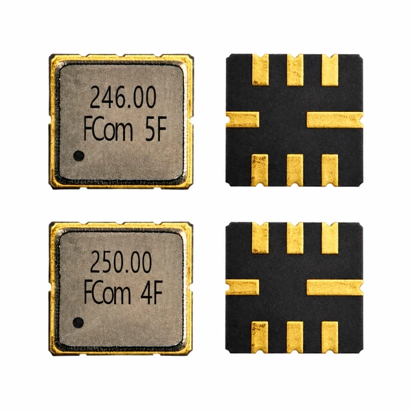
Choose by frequency and interface
Two models with distinct design requirements
Check the bandwidth definition and matching conditions before comparing loss. Both models are covered in the combined FCom document, one page per model.
SAW Filter · 246 MHz
FSF-5050-246M
246 MHz
External matching required
- 1 dB bandwidth
- 200 kHz min. / 350 kHz typ.
- 3 dB bandwidth
- 0.5 MHz typ.
- Minimum insertion loss, ILmin
- 2.1 dB typ. / 3.4 dB max. incl. real matching losses
- Operating temperature
- −20 to +70 °C
SAW Filter · 250 MHz
FSF-5050-250M
250 MHz
50 Ω source/load test terminations
- Specified passband
- 249.9–250.9 MHz
- 3 dB bandwidth
- — (not specified)
- Insertion loss
- 2.05 dB typ. / 3.8 dB max. over specified passband
- Operating temperature
- −40 to +85 °C
Compare definitions before numbers. 246M minimum insertion loss and 250M passband insertion loss describe different conditions. Their bandwidth definitions, matching needs and operating limits also differ; a shared package does not establish interchangeability.
Six key parameters per model
Electrical specifications
Separate tables preserve each model’s measurement definitions. Full stopband limits and further conditions remain in the combined product document.
Scroll horizontally to view all columns.
FSF-5050-246M
| Parameter | Min. | Typ. | Max. | Unit | Definition / condition |
|---|---|---|---|---|---|
| Center frequency | — | 246.0 | — | MHz | Stated center frequency; no frequency-tolerance limit is added. |
| 1 dB bandwidth | 200 | 350 | — | kHz | Keep the 1 dB definition separate from the 3 dB bandwidth. |
| 3 dB bandwidth | — | 0.5 | — | MHz | Typical value; no minimum or maximum is stated. |
| Minimum insertion loss, ILmin | — | 2.1 | 3.4 | dB | Includes losses in real matching components; not a full-passband insertion-loss specification. |
| Passband relative to ILmin | 245.9–246.1 | MHz | 0.5 dB typ. / 1.5 dB max. relative to ILmin; ideal simulated matching. Not relabeled as amplitude ripple. | ||
| Operating temperature | −20 | — | +70 | °C | Operating limits; storage limits are separate. |
Ideal-match ILmin is 1.9 dB typ. / 3.2 dB max., excluding matching-element losses. The passband and stopband values relative to ILmin use ideal simulated matching. Do not combine those values with real-match ILmin to infer an unqualified passband-loss limit.
FSF-5050-250M
| Parameter | Min. | Typ. | Max. | Unit | Definition / condition |
|---|---|---|---|---|---|
| Center frequency | — | 250.0 | — | MHz | Stated center frequency; no frequency-tolerance limit is added. |
| Specified passband | 249.9–250.9 | MHz | Interval for insertion loss and amplitude ripple; not a 3 dB bandwidth. | ||
| Insertion loss | — | 2.05 | 3.8 | dB | Over 249.9–250.9 MHz, with 50 Ω source/load test terminations. |
| Amplitude ripple | — | 0.13 | 1.8 | dB | Over 249.9–250.9 MHz. |
| Operating temperature | −40 | — | +85 | °C | Operating limits; do not apply this range to 246M. |
| Source / load test termination | 50 / 50 | Ω | Direct test connection; evaluate the actual system interface. | ||
The 249.9–250.9 MHz interval is reproduced as specified; it is not symmetric about the stated 250 MHz center frequency. Its 1 MHz span must not be labeled a 3 dB bandwidth. Stopband attenuation is referenced to 0 dB.
No electrical-characteristic test temperature is stated in the supplied FCom document. Operating ranges do not make every typical value a guaranteed limit throughout that range. “—” means not specified.
Typical Applications
VHF signal selection and IF filtering
VHF receiver filtering
Select the center frequency and bandwidth definition that fit the receiver’s wanted-signal band.
RF front-end selection
Check wanted-signal loss and blocker rejection under the selected model’s matching and termination conditions.
Superheterodyne IF stages
Evaluate the filter between the actual preceding and following IF stages, including any required matching networks.
Application example only. This is not a validated circuit or pin-routing diagram.
Design-in essentials
Keep matching conditions with the specification
246M: plan the matching network
The test source and load are 50 Ω, but the ideal model gives 2195 Ω ∥ 1.9 pF at the input and 2915 Ω ∥ 1.68 pF at the output, both at Fc.
External matching is required. The supplied ideal model lists series inductance of 212 nH at the input and 245 nH at the output, with 0 pF ideal shunt capacitance at each port. These simulation values are not a finalized production component list.
Evaluate the real components, parasitics and PCB conditions. Maximum RF input: 10 dBm. Maximum DC voltage: 0 V.
250M: verify the 50 Ω interface
The document uses 50 Ω source and load terminations with a direct test connection. Evaluate the intended source, load and PCB fixture before assuming the same response in your system.
Assess insertion loss and ripple across the exact 249.9–250.9 MHz interval, and use the PDF’s 0 dB-referenced stopband limits at the relevant blocker frequencies.
Maximum RF input: 10 dBm. Maximum DC voltage: 5 V. Maximum ratings are limits, not recommended operating targets.
Shared mechanical format
Package & pin assignment
5.0 × 5.0 mm · 1.5 mm maximum height · 8-pad SMD
The supplied FCom drawings show these dimensions and pin functions for both models. Confirm pad orientation and signal-port assignment using the applicable drawing before PCB release, particularly for the unequal 246M input/output matching requirements.
For other pin configurations, contact FCom.
| Pin(s) | Function |
|---|---|
| 2 | Input / Output |
| 6 | Input / Output |
| 1, 3, 5, 7 | Ground |
| 4, 8 | Case Ground |
The FCom table labels both signal pins Input/Output; this does not establish identical impedances or interchangeable matching networks.
Selection and design-in support
Share your signal and interface requirements
Include the chosen frequency, bandwidth definition, source/load requirements, temperature range, sample quantity and estimated usage. For 246M, include the intended matching approach; for either model, add blocker frequencies and rejection targets where relevant.
Confirm the applicable specification, signal-port orientation and complete ordering code with FCom before ordering.
Engineering Questions
Frequently asked questions
How should I choose between 246M and 250M?
Start with the required center frequency, bandwidth definition and interface. 246M provides specified 1 dB and 3 dB bandwidths and requires external matching. 250M specifies insertion loss and amplitude ripple over 249.9–250.9 MHz with 50 Ω source/load test terminations. Their loss definitions and temperature ranges differ; the shared package does not establish interchangeability.
Can 246M be connected as a directly matched 50 Ω filter?
The supplied document requires external matching for 246M. Its 50 Ω values describe the test source and load. The ideal model gives input impedance 2195 Ω in parallel with 1.9 pF and output impedance 2915 Ω in parallel with 1.68 pF at the center frequency; these are not 50 Ω device-port specifications.
Why does 246M have two minimum insertion-loss values?
The 2.1 dB typical / 3.4 dB maximum values include losses in real matching components. The 1.9 dB typical / 3.2 dB maximum values use ideal simulated matching and exclude matching-element losses. Passband and stopband values relative to ILmin use the ideal matching condition. Do not add values from these different conditions to construct an unqualified passband-loss limit.
What bandwidth is specified for 250M?
The document gives 249.9–250.9 MHz as the interval for insertion loss and amplitude ripple, a span of 1 MHz. It does not specify a 3 dB bandwidth. Retain these endpoints as stated; the interval is not symmetric about the stated 250 MHz center frequency.
Do the two models have the same operating and DC limits?
No. 246M is specified for −20 to +70°C operation and a maximum DC voltage of 0 V. 250M is specified for −40 to +85°C operation and a maximum DC voltage of 5 V. Both list 10 dBm maximum RF input power. Maximum ratings are limits, not recommended operating targets.
What information is needed for selection and ordering?
Provide the selected model or center frequency, required bandwidth and attenuation threshold, source/load requirements, operating temperature, sample quantity and estimated usage. For 246M, include the matching approach and applicable PCB conditions. Confirm signal-port orientation and the full ordering code with FCom before ordering.