
High-fundamental reference clocks for optical and networking systems
FCO-6L-UJ Ultra-Low-Jitter Differential Crystal Oscillator
100–220 MHz · 2016 six-pad SMD
The FCO-6L-UJ uses high-fundamental quartz technology to provide low-phase-noise reference clocks for compatible 400G, 800G and 1.6T optical modules. This compact 2016 series offers LVDS, LVPECL or HCSL output, with 40 fs typical RMS phase jitter at 3.3 V, integrated from 12 kHz to 20 MHz.
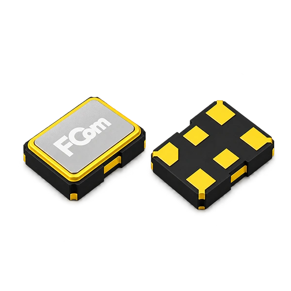
Body: 2.05 × 1.65 × 0.70 mm, each ±0.10 mm.
Use the mechanical drawing for footprint design.
FCO-6L-UJ uses the same high-fundamental technology as FCO-2LH. High-frequency fundamental-mode operation supports low source phase noise and low integrated jitter. Select the reference frequency, interface and stability grade against the optical DSP or SerDes requirements, including its phase-noise mask and jitter integration bandwidth.
Key Features
A compact differential reference-clock platform with standard frequencies of 100 MHz, 125 MHz, 156.25 MHz and 212.5 MHz, three output interfaces and stability grades matched to the operating-temperature range.
Low RMS phase jitter
40 fs typ.
Typical RMS phase jitter at 3.3 V, integrated from 12 kHz to 20 MHz under the specified test conditions.
Maximum limits at 3.3 V: 70 fs for LVDS and HCSL; 80 fs for LVPECL.
Frequency stability options
±50 ppm max.
Overall stability grade available over −40 to +105°C. Recommended parts on this page use the ±50 ppm grade.
Additional options include ±25 ppm over −40 to +85°C and ±20 ppm over −20 to +70°C.
Compact differential interface
2.0 × 1.6 mm nom.
2016 six-pad SMD package with complementary outputs and tri-state enable/disable control.
LVDS and HCSL supplies: 1.8 / 2.5 / 3.3 V. LVPECL supplies: 2.5 / 3.3 V.
Typical Applications
Recommended FCom part numbers for compatible optical, networking and HCSL clock inputs. All listed parts use a 3.3 V supply and ±50 ppm overall stability. Differences in frequency, output interface or temperature range are shown after each part number.
400G, 800G and 1.6T Optical Modules
A 156.25 MHz reference for optical DSP and SerDes inputs that accept this frequency and the specified clock-noise limits. High-fundamental quartz technology supports low source phase noise, while the 2016 package accommodates placement close to the receiver.
Recommend Parts
Design consideration. Select LVDS where the receiver accepts its output levels; its supply-current limit is 20 mA. Confirm that ±50 ppm stability and 70 fs maximum LVDS jitter, or 80 fs maximum LVPECL jitter, meet the receiver budget. The −40 to +105°C grade supports elevated local operating temperatures.
Switch, SerDes and FPGA Reference Clocks
Fixed-frequency references for compatible switch ASICs, FPGA transceivers and clock-distribution inputs. The options below use LVDS output and the −40 to +105°C temperature grade; select the frequency required by the receiving device.
Recommend Parts
Design consideration. The specified LVDS load is 100 Ω across the differential outputs. Review receiver common-mode range and coupling requirements, and include buffer or synthesizer noise in the clock budget at the receiving input.
100 MHz HCSL Reference Clocks
A 100 MHz HCSL source for evaluating compatible PCIe reference-clock trees and other HCSL inputs. The listed 3.3 V configurations provide a 38 mA maximum supply current and a specified load of 50 Ω from each output to ground.
Recommend Parts
Design consideration. PCIe qualification requires the applicable generation-specific jitter filtering, clock architecture and electrical tests. The oscillator’s 12 kHz–20 MHz RMS jitter figure alone does not establish PCIe compliance.
Optical and Networking Evaluation Platforms
A 156.25 MHz reference for DSP evaluation boards, network equipment and laboratory characterization. The options below share the −40 to +85°C temperature grade and allow selection of LVDS, LVPECL or HCSL to match the test platform.
Recommend Parts
Design consideration. Evaluate phase noise, integrated jitter, differential waveforms and supply-noise sensitivity with the intended termination. Use consistent supply, load, temperature and integration bandwidth when comparing measurements.
Select a recommended part number to request pricing, samples or technical support. For other supply-voltage requirements, including 1.8 V or 2.5 V LVDS/HCSL and 2.5 V LVPECL options, please contact our sales team.
Frequently Asked Questions
Does FCO-6L-UJ use the same high-fundamental technology as FCO-2LH?
Yes. FCO-6L-UJ uses the same high-fundamental quartz technology as FCO-2LH. Fundamental-mode operation at high frequency supports low source phase noise and low integrated jitter for compatible optical DSP, SerDes and clock-synthesis reference inputs. FCO-6L-UJ has its own frequency, jitter, stability and interface specifications.
Which frequencies are available?
The series covers 100–220 MHz. Standard fixed-frequency options are 100 MHz, 125 MHz, 156.25 MHz and 212.5 MHz. Each ordered part has one specified output frequency. Contact FCom for other frequencies within the published range; select the nominal frequency required by the receiver.
Is 40 fs a typical value or a maximum limit?
40 fs is the typical RMS phase-jitter value at 3.3 V, integrated from 12 kHz to 20 MHz. The maximum is 70 fs for LVDS and HCSL, and 80 fs for LVPECL. Typical values are not maximum limits.
The datasheet lists 50 fs typical and 80 fs maximum in the 1.8 V HCSL column, while its jitter measurement note specifies 3.3 V. For lower-voltage designs, confirm the applicable measurement conditions and limits in the approved configuration specification. The published test environment is 25 ±5°C and 40–70% relative humidity.
How should stability and temperature grades be selected?
The recommended part numbers on this page use the ±50 ppm overall stability grade, code F, with −40 to +85°C, code Y, or −40 to +105°C, code U. The stability table also lists ±25 ppm over −40 to +85°C and ±20 ppm over −20 to +70°C.
The ±20 ppm option over −40 to +85°C is conditional. Neither ±20 ppm nor ±25 ppm is listed for −40 to +105°C. At −40 to +125°C, ±100 ppm is available and ±50 ppm is conditional; contact FCom for selection review.
Overall stability includes calibration at 25°C, operating-temperature range, input-voltage variation, load variation, first-year aging, shock and vibration. The separate aging specification is ±3 ppm for the first year at 25°C.
Which supply options and current limits are specified?
LVDS and HCSL are available with nominal supplies of 1.8 V, 2.5 V or 3.3 V. LVPECL supports 2.5 V or 3.3 V. Maximum supply current is 20 mA for LVDS and 60 mA for LVPECL. HCSL is specified at 38 mA maximum for 2.5 V or 3.3 V, and 32 mA maximum for 1.8 V.
The series specifies a maximum start-up time of 2 ms, a maximum standby current of 10 µA and a 45–55% duty cycle. Supply voltage and output interface are selected at ordering.
Which parts should be evaluated for 800G and 1.6T optical modules?
For a receiver that accepts a 156.25 MHz LVDS reference, FCO6L33DFYUJ-156.25MHz specifies 3.3 V, ±50 ppm and −40 to +85°C. FCO6L33DFUUJ-156.25MHz extends the operating-temperature range to −40 to +105°C. FCO6L33PFUUJ-156.25MHz provides the LVPECL interface at the same extended temperature grade.
Final selection depends on the optical DSP or SerDes reference frequency, permitted frequency error, phase-noise mask, jitter bandwidth and electrical input requirements. Line rate alone does not determine the oscillator configuration. A receiver requiring a frequency above 220 MHz needs a separately specified oscillator series.
What termination, decoupling and enable conditions apply?
The specified LVDS load is 100 Ω across OUT and OUTN. LVPECL uses 50 Ω from each output to VDD − 2 V; HCSL uses 50 Ω from each output to ground. Select coupling and termination to satisfy both the oscillator and receiver requirements.
Place a 0.1 µF bypass capacitor close to the VDD and ground connections. The tri-state control thresholds are VIH ≥0.7 × VDD for enable and VIL ≤0.3 × VDD for disable. Use the approved package drawing and pin assignment for PCB design.
What are the package dimensions?
FCO-6L-UJ uses a nominal 2016, 2.0 × 1.6 mm, six-pad SMD package. The mechanical drawing specifies 2.05 ±0.10 mm length, 1.65 ±0.10 mm width and 0.70 ±0.10 mm height. Use the drawing dimensions and recommended land pattern when designing the PCB footprint.