
High-fundamental reference clocks for optical transceivers
FCO-2LH Low-Jitter Differential Crystal Oscillator
285 MHz / 312.5 MHz · 2520 six-pad SMD
The FCO-2LH is a high-fundamental quartz oscillator designed to provide low-phase-noise differential reference clocks for 800G and 1.6T optical transceivers. Fixed 285 MHz and 312.5 MHz configurations combine LVDS or LVPECL output with 40 fs maximum RMS phase jitter (12 kHz–20 MHz), ±20 ppm overall frequency stability and a compact 2520 package.
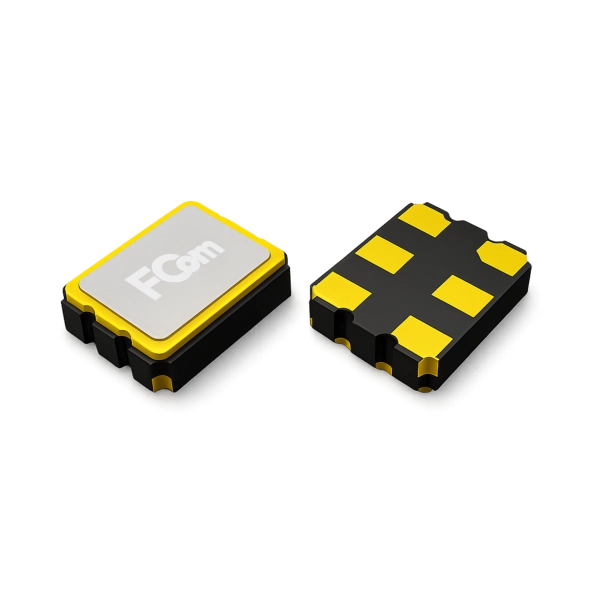
Package orientation is defined in the mechanical drawing.
High-frequency fundamental-mode operation supports low source phase noise and low integrated jitter. The resulting reference is suited to compatible optical DSP, SerDes and clock-synthesis inputs. Device selection is based on the receiving circuit’s reference frequency, phase-noise mask, jitter integration bandwidth and electrical interface.
Key Features
A compact differential reference-clock platform combining low integrated jitter, tight frequency stability and operating-temperature options for optical communication equipment.
Low RMS phase jitter
40 fs max.
Maximum RMS phase jitter of 40 fs, integrated from 12 kHz to 20 MHz under the specified measurement conditions.
Available at fixed output frequencies of 285 MHz and 312.5 MHz.
Overall frequency stability
±20 ppm max.
The overall stability grade includes the specified initial-frequency, temperature, supply-voltage and aging contributions.
Operating-temperature options: −40 to +85°C and −40 to +105°C.
Differential output interface
2.5 × 2.0 mm nom.
2520 six-pad SMD package with complementary outputs and a dedicated output-enable input.
LVDS supply options: 1.8 / 2.5 / 3.3 V. LVPECL supply options: 2.5 / 3.3 V.
Typical Applications
Recommended FCom part numbers for compatible optical and networking clock inputs. The listed parts use a 3.3 V supply. Frequency, output interface and temperature grade are selected according to the receiving device and the system operating conditions.
800G Optical Transceivers
A differential reference for compatible 800G optical DSP and SerDes inputs. Low oscillator jitter limits the source contribution to the clock budget, while the 2520 package supports placement close to the receiving device.
Recommend Parts
Design consideration. LVDS is recommended where the receiver accepts its swing and common-mode range. The FCO-2LH LVDS supply-current limit is 40 mA; LVPECL configurations are available where required by the receiver.
1.6T Optical Transceivers
A reference-clock option for 1.6T architectures that accept a 312.5 MHz differential input. Selection addresses the DSP phase-noise mask, clock-distribution noise and the thermal conditions at the oscillator location.
Recommend Parts
Design consideration. The extended-temperature grade is recommended for designs with elevated local operating temperatures. Architectures requiring 625 MHz need a separately specified oscillator; the listed FCO-2LH configurations are 285 MHz and 312.5 MHz.
Switch, SerDes and FPGA Reference Clocks
Fixed references for compatible switch ASICs, FPGA transceivers and clock-distribution inputs. The selected frequency must match the device reference-clock architecture, with output levels, coupling and termination reviewed together.
Recommend Parts
Design consideration. Clock buffers and synthesizers contribute additional noise. Compliance is assessed at the receiving clock input using the device-specific phase-noise and jitter limits.
Optical-Module Evaluation Platforms
A reference source for DSP evaluation boards and optical-module characterization. Evaluation uses the intended operating frequency and electrical interface, with controlled supply, loading and measurement bandwidth for repeatable results.
Recommend Parts
Design consideration. Recommended evaluation includes phase noise, integrated RMS jitter, differential waveform and supply-noise sensitivity. The source specification applies to the oscillator under its specified conditions; distribution circuitry is evaluated separately.
Select a recommended part number to request pricing, samples or technical support. For other supply-voltage requirements, including 1.8 V LVDS and 2.5 V LVDS/LVPECL options, please contact our sales team.
Frequently Asked Questions
What is the operating principle of FCO-2LH?
FCO-2LH uses a high-fundamental quartz resonator operating in its fundamental mode at high frequency. This architecture supports low source phase noise and low integrated jitter for compatible optical DSP, SerDes and clock-synthesis reference inputs.
Which configuration is recommended for 800G and 1.6T optical modules?
For compatible 312.5 MHz LVDS clock inputs, FCO2LH33DCYYUJ-312.5MHz specifies 3.3 V operation over −40 to +85°C, while FCO2LH33DCUYUJ-312.5MHz specifies the −40 to +105°C option. For LVPECL inputs requiring the extended-temperature grade, FCO2LH33PCUYUJ-312.5MHz is listed. Final selection follows the receiver’s electrical and clock-noise requirements.
Which frequency and supply configurations are available?
Fixed 285 MHz and 312.5 MHz configurations are available. LVDS nominal supply options are 1.8 V, 2.5 V and 3.3 V; LVPECL options are 2.5 V and 3.3 V. Frequency, interface, supply and temperature grade are specified at ordering. A design requiring a different reference frequency requires a separate product specification.
What measurement conditions apply to the jitter specification?
The maximum RMS phase-jitter specification is 40 fs, integrated from 12 kHz to 20 MHz under the datasheet test conditions. The LVDS measurement note identifies a 3.3 V supply. Comparison and qualification use consistent bandwidth, supply, output load and temperature conditions, together with the receiving device’s phase-noise mask.
What is included in the overall frequency stability grade?
The ±20 ppm overall grade includes the specified initial-frequency, temperature, supply-voltage and aging contributions. Available operating-temperature ranges are −40 to +85°C and −40 to +105°C. The approved configuration specification defines the applicable limits and conditions.
What output-termination conditions are specified?
The LVDS reference load is 100 Ω across OUT and OUTN. The LVPECL reference load is 50 Ω from each output to VDD − 2 V. The final coupling and termination network is determined by the receiver input swing and common-mode range. Local supply decoupling is placed adjacent to the oscillator supply and ground connections.